Semiconductor device, method of manufacture thereof and semiconductor integrated circuit

a semiconductor and integrated circuit technology, applied in the field of element isolation techniques, can solve the problems of increasing the formation of the pn junction, and the increase of the parasitic capacitance of the source and drain region, so as to reduce the parasitic capacitance of the parasitic junction and reduce the parasitic capacitance of the wiring

Inactive Publication Date: 2008-10-07
RENESAS ELECTRONICS CORP
View PDF15 Cites 1 Cited by
  • Summary
  • Abstract
  • Description
  • Claims
  • Application Information

AI Technical Summary

Benefits of technology

[0009]It is an object of the present invention to provide a technique of reducing parasitic junction capacitance of a source region and a drain region, and reducing parasitic capacitance of wiring.
[0011]The nonexistence of an impurity layer on the second direction side of the source and drain regions allows a reduction in parasitic junction capacitance of these regions. In addition, parasitic capacitance of wiring installed on the opposite side to the insulating layer is reduced between a source region of one transistor and a drain region of another transistor adjacent in the second direction to the one transistor.
[0015]The semiconductor layer is etched to a depth that does not reach the insulating layer with the silicon nitride film as a mask, and then part of the etched semiconductor layer is further etched to a depth that reaches the insulating layer, with the photoresist and the silicon nitride film as a mask. Thereafter, the insulating film is buried in the etched portions to form the element isolation insulating film. As a result, an element isolation insulating film that does not reach the insulating layer and an element isolation insulating film that reaches the insulating layer can be formed. In addition, since both of the photoresist and the silicon nitride film are used as a mask during the etching to a depth that reaches the insulating layer, the element isolation insulating film that reaches the insulating layer will not be expanded accidentally even when patterning misalignment of the photoresist occurs.

Problems solved by technology

The simple separation of the insulating film for element isolation from the buried insulating layer, however, will result in a pn junction being formed and resultant capacitance being generated between the source and drain regions and the impurity layer left between the insulating film for element isolation and the buried insulating layer.
This causes an increase in parasitic capacitance of the source and drain regions.
That causes the impurity layer left between the insulating film for element isolation and the buried insulating layer to contribute to an increase in parasitic capacitance of the wiring.

Method used


Image

  • Semiconductor device, method of manufacture thereof and semiconductor integrated circuit
  • Semiconductor device, method of manufacture thereof and semiconductor integrated circuit
  • Semiconductor device, method of manufacture thereof and semiconductor integrated circuit

Examples


first preferred embodiment

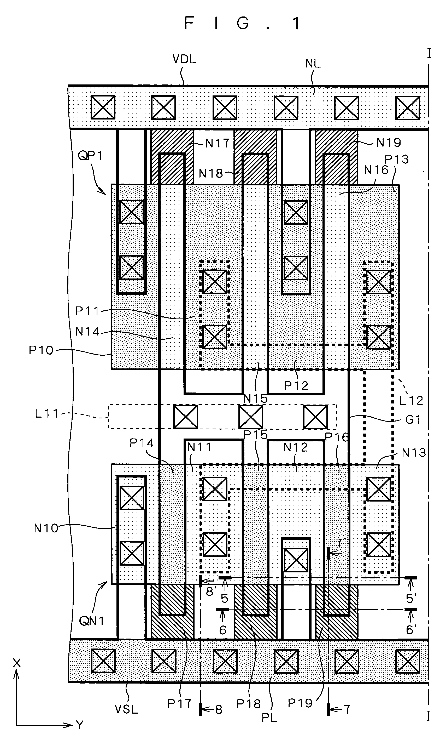
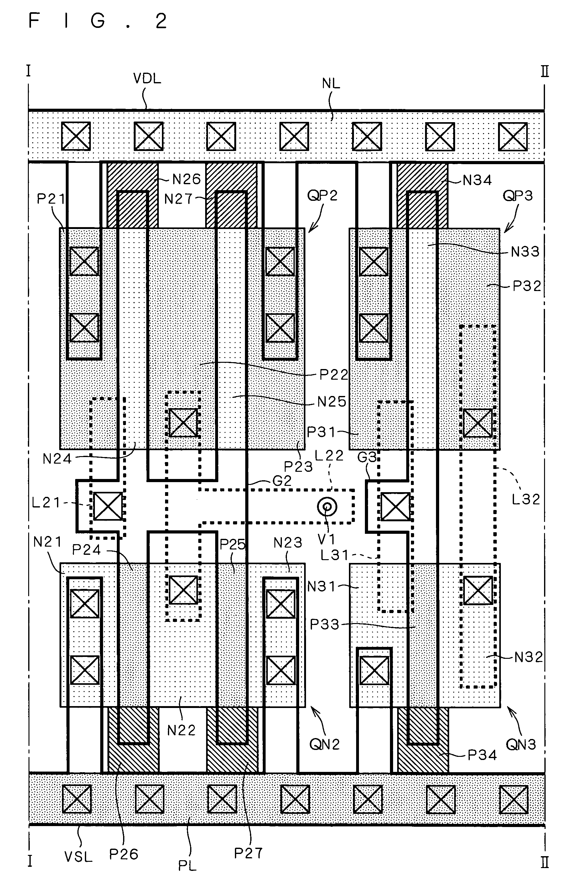
[0040]FIGS. 1 to 3 are plan views together illustrating an element isolation technique according to a first preferred embodiment of the present invention. FIG. 4 is a schematic view depicting connections of FIGS. 1 to 3. FIGS. 1 and 2 are connected along an imaginary line I-I, and FIGS. 2 and 3 along an imaginary line II-II, to form the whole of the plan views.

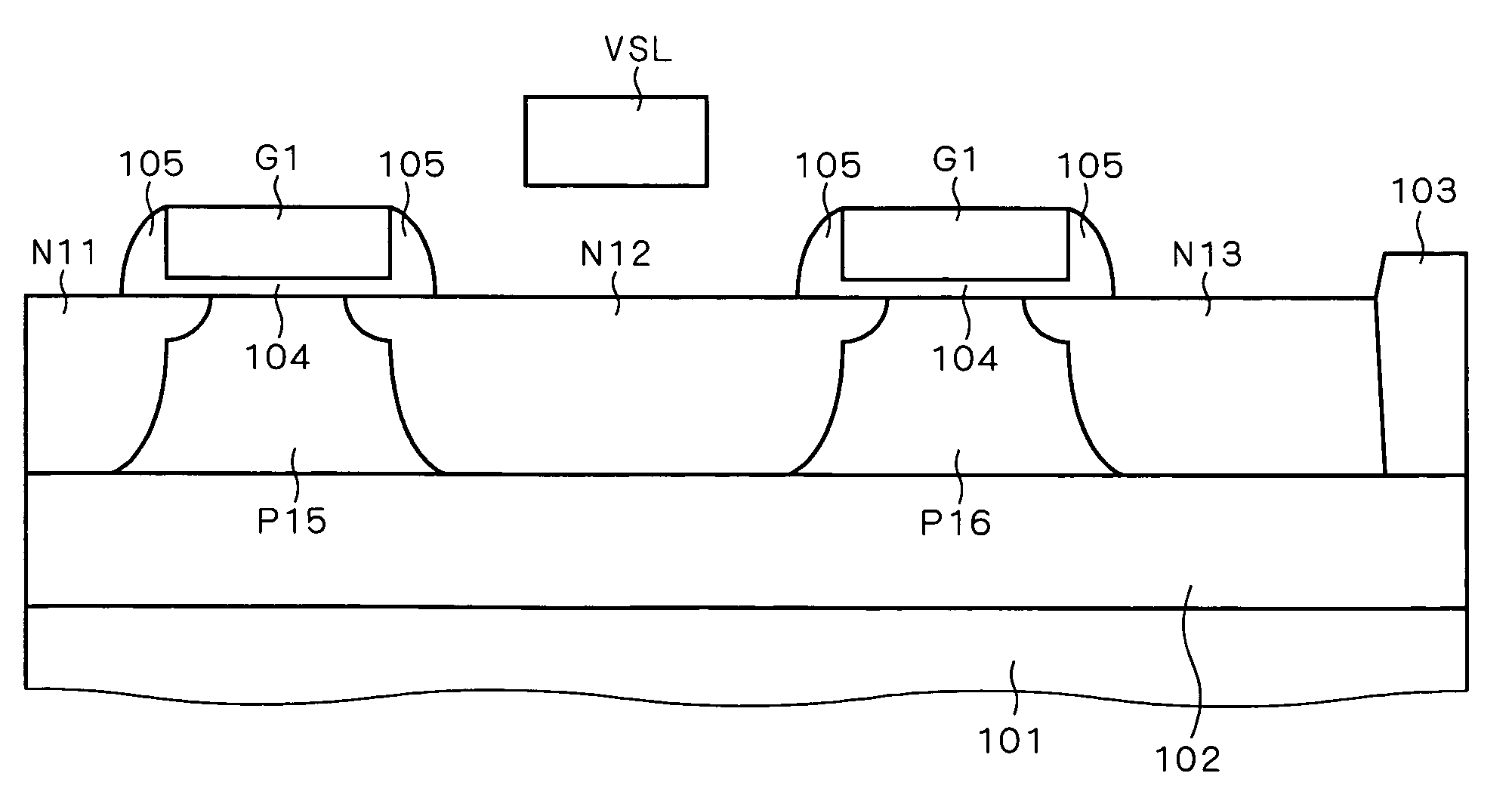
[0041]In FIGS. 1 to 3, a gate array is illustrated in which a low potential line VSL, a group of NMOS transistors, a group of PMOS transistors, and a high potential line VDL are arranged in this order with respect to a direction (positive direction of an X direction) from the lower part to the upper part in the drawings. The low potential line, the high potential line, the group of NMOS transistors and the group of PMOS transistors are all formed in an SOI substrate (not shown). The application to a gate array should not be construed as limiting the present invention.

[0042]Each of the low potential line VSL and the high potent...

second preferred embodiment

[0085]As illustrated in FIG. 3, the gate width of the transistors QP4 and QN4 is narrower than the gate widths of the transistors QP1 to QP3 and QN1 to QN3. In order to reduce the resistance of the gate electrode G4 that is used both in the transistors QP4 and QN4, it is desirable that the transistors QP4 and QN4 be arranged close to each other with respect to the X direction.

[0086]Such arrangement, however, causes the N-type impurity layer N44 and the P-type impurity layer P44 in the PTI regions to increase in length in the X direction. A current flows in the X direction through the N-type impurity layer N44 that is interposed between and adjacently to the N-type impurity layers NL and N43. The same thing occurs in the P-type impurity layer P44. It is therefore desirable from the viewpoint of reducing the resistance of the impurity regions for fixing the body region potentials that the width with respect to the Y direction of the PTI regions be increased.

[0087]However, the simple w...

third preferred embodiment

[0103]An LSI (large scale integrated circuit) is often designed and manufactured by being divided into a plurality of blocks. For example, the design and manufacture are often conducted by mixing a block (hereafter called a “Type I block”) forming a circuit of relatively low degree of design freedom such as a cell base and a gate array used to form a logic circuit, and a block (hereafter called a “Type II block”) forming a circuit of relatively high degree of design freedom such as a SRAM (static RAM), a PLL (phase locked loop), an ADC (analog / digital converter), a DAC (digital / analog converter) and an I / O (input / output circuit). This applies to when designing and manufacturing an LSI on an SOI substrate as well.

[0104]When designing and manufacturing an LSI on an SOI substrate, it is better to apply the technique of limiting PTI regions to predetermined regions as in the present invention to the Type I block having the lower degree of design freedom than the Type II block. This is b...


PUM


Abstract

An FTI structure is employed in an isolation region making contact in a Y direction with a P-type impurity region serving as a drain region of a PMOS transistor. First, second and third N-type impurity layers serving as body regions are connected to a high potential line via fourth, fifth and sixth N-type impurity layers, respectively, and further via a seventh N-type impurity layer. The fourth to sixth N-type impurity layers are provided between an insulating layer of an SOI substrate and an element isolation insulating film in a PTI region.

Description

BACKGROUND OF THE INVENTION[0001]1. Field of the Invention[0002]The present invention relates to element isolation techniques, and especially to element isolation regarding MIS (Metal Insulator Semiconductor) transistors formed on an SOI (Silicon On Insulator) substrate.[0003]2. Description of the Background Art[0004]It is known that an insulating film is used in an element isolation technique for isolating a plurality of MIS transistors (MOS transistors, for example). The insulating film for element isolation is formed by a process from the surface of a semiconductor substrate on which the MOS transistors are to be formed.[0005]In the so-called bulk type MOS transistor, namely a MOS transistor including a source region and a drain region by forming high concentration impurity layers restrictively in the surface of a semiconductor substrate, a region left between the source and drain regions in the semiconductor substrate is connected to the surface of the semiconductor substrate as...

Claims


Application Information

Patent Timeline
Patent Type & Authority Patents(United States)
IPC IPC(8): H01L29/93
CPCH01L21/761H01L21/76281H01L21/84H01L27/0207H01L27/11807H01L27/1203G02F1/1309G01N21/8803G02F2203/69
Inventor KANAMOTO, TOSHIKIYOSHIDA, MASUMIWATANABE, TETSUYAIPPOUSHI, TAKASHI
Owner RENESAS ELECTRONICS CORP
Why Eureka
Try Eureka