Semiconductor device and method of manufacturing a semiconductor device

a semiconductor device and semiconductor technology, applied in the field of semiconductor devices and manufacturing methods, can solve the problems of trade-off between these two parasitic components, and achieve the effects of reducing the parasitic junction capacitance, reducing the collector-base capacitance, and increasing the maximum oscillation frequency of the semiconductor devi

Active Publication Date: 2020-11-03
NXP USA INC
View PDF12 Cites 0 Cited by
  • Summary
  • Abstract
  • Description
  • Claims
  • Application Information

AI Technical Summary

Benefits of technology

[0014]By providing a second dielectric spacer, separating the base link region from at least the periphery of the collector region and extending laterally beyond the first dielectric spacer to underlie said emitter window region, the present invention may further reduce the parasitic junction capacitance between the base and collector, which in turn may lead to an increase in the maximum oscillation frequency of the semiconductor device. In particular, the present invention may enable the base link region or base link structure to be formed substantially fully over a dielectric instead of the collector region, thereby reducing the collector-base capacitance while maintaining low base resistance. Together, the first dielectric spacer and the second dielectric spacer may form an L-shaped spacer with a discontinuous vertical portion.
[0015]The present invention also enables the base link region to be formed over a dielectric region only after a portion of a selective-epi collector region has been grown, by separating growth of the selective-epi collector region and formation of the intrinsic base region into two separate steps. Since the base link region may be grown during growth of the intrinsic base region, the base link region may be narrower compared to that obtained when the selective-epi collector region and the intrinsic base region are grown in a single process. This may also help to ensure that the base link region is fully over the second dielectric spacer rather than being partially formed over the collector region.
[0027]The conductive layer may improve the electrical coupling between the intrinsic base region and the extrinsic base region, thereby reducing the base resistance.

Problems solved by technology

Device fabrication usually results in a trade-off between these two parasitic components.

Method used


Image

  • Semiconductor device and method of manufacturing a semiconductor device
  • Semiconductor device and method of manufacturing a semiconductor device
  • Semiconductor device and method of manufacturing a semiconductor device

Examples


first embodiment

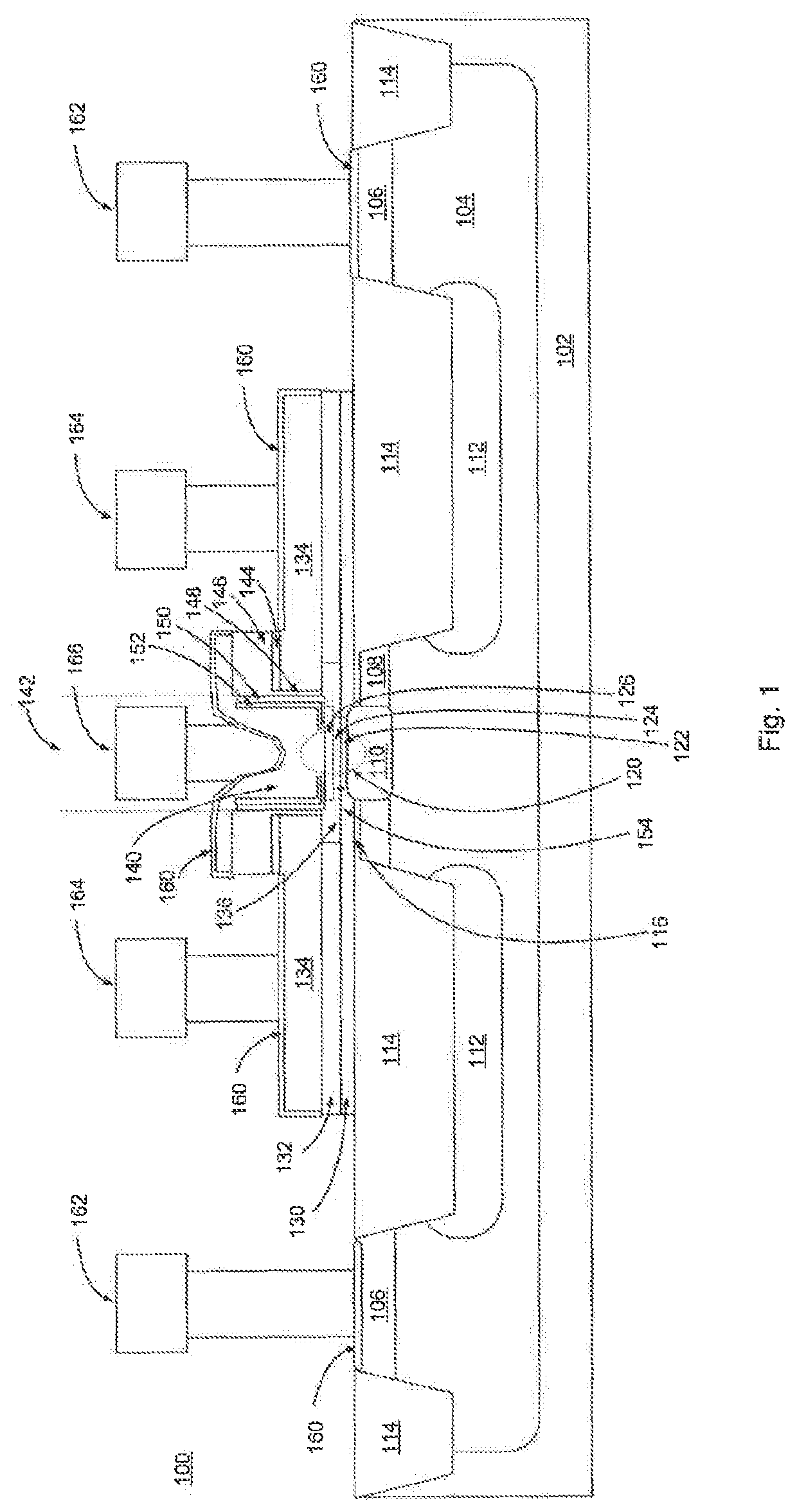
[0061]FIG. 1 shows a schematic cross-sectional view of a semiconductor device 100 according to the present invention. In this embodiment, semiconductor device 100 is in the form of a selective-epi base silicon germanium (SiGe) npn heterojunction bipolar transistor (HBT). However, this is not intended to be limiting and persons skilled in the art will understand that, by appropriate substitution of semiconductor regions of opposite conductivity type and / or use of silicon or other semiconductor materials, pnp and other types of semiconductor devices can be provided in accordance with the present invention, on silicon or other semiconductor substrates. The cross-section of the semiconductor device 100 illustrated in FIG. 1 is symmetric about a central vertical line, and accordingly some elements are labelled on only one side of the cross-section in order to improve clarity.

[0062]Semiconductor device 100 comprises a substrate 102, in the form of a p−-doped silicon substrate, in which co...

second embodiment

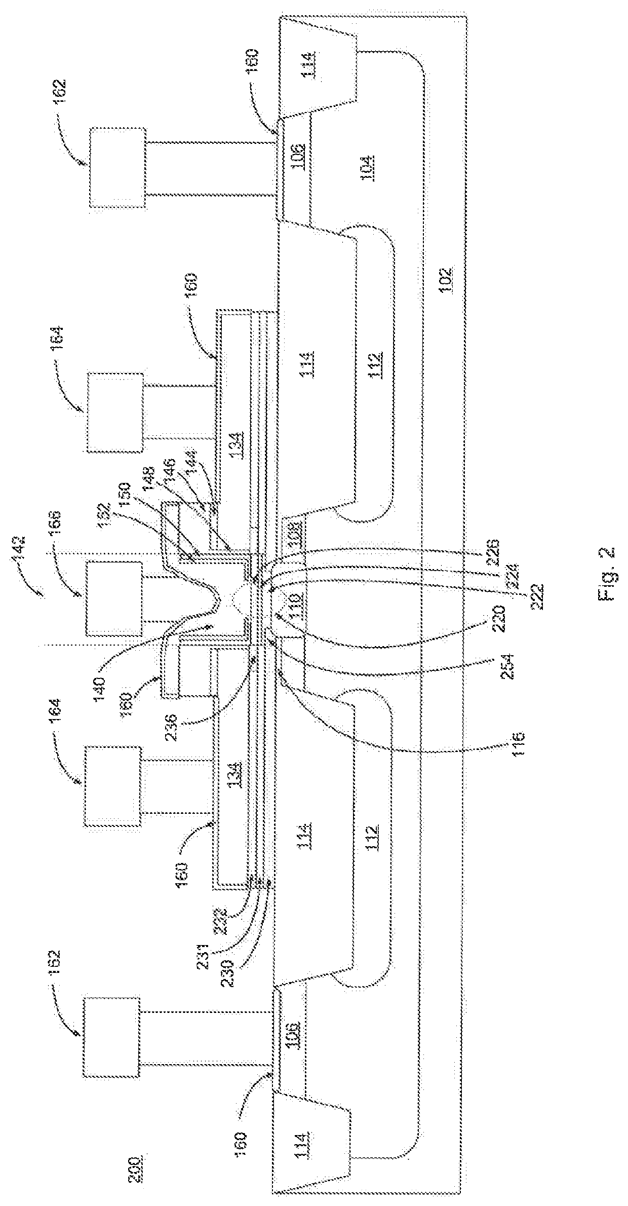
[0070]FIG. 2 shows a schematic cross-sectional view of a semiconductor device 200, in the form of a selective-epi base silicon germanium (SiGe) npn heterojunction bipolar transistor (HBT), according to the invention. Elements shown in FIG. 2 which correspond to elements described above with reference to FIG. 1 are indicated by the same reference numbers (where the elements are substantially the same), or by reference numbers increased by 100 (where the elements may differ). Semiconductor device 200 differs from semiconductor device 100 in that it includes a conductive layer 231 in the form of a further polysilicon layer 231 between the lower dielectric layer 230 and the upper dielectric layer 232. The base link region 236 extends between the extrinsic base region 134 and the conductive layer 231, and couples the intrinsic base region 224 to the extrinsic base region 134 via the conductive layer 231.

third embodiment

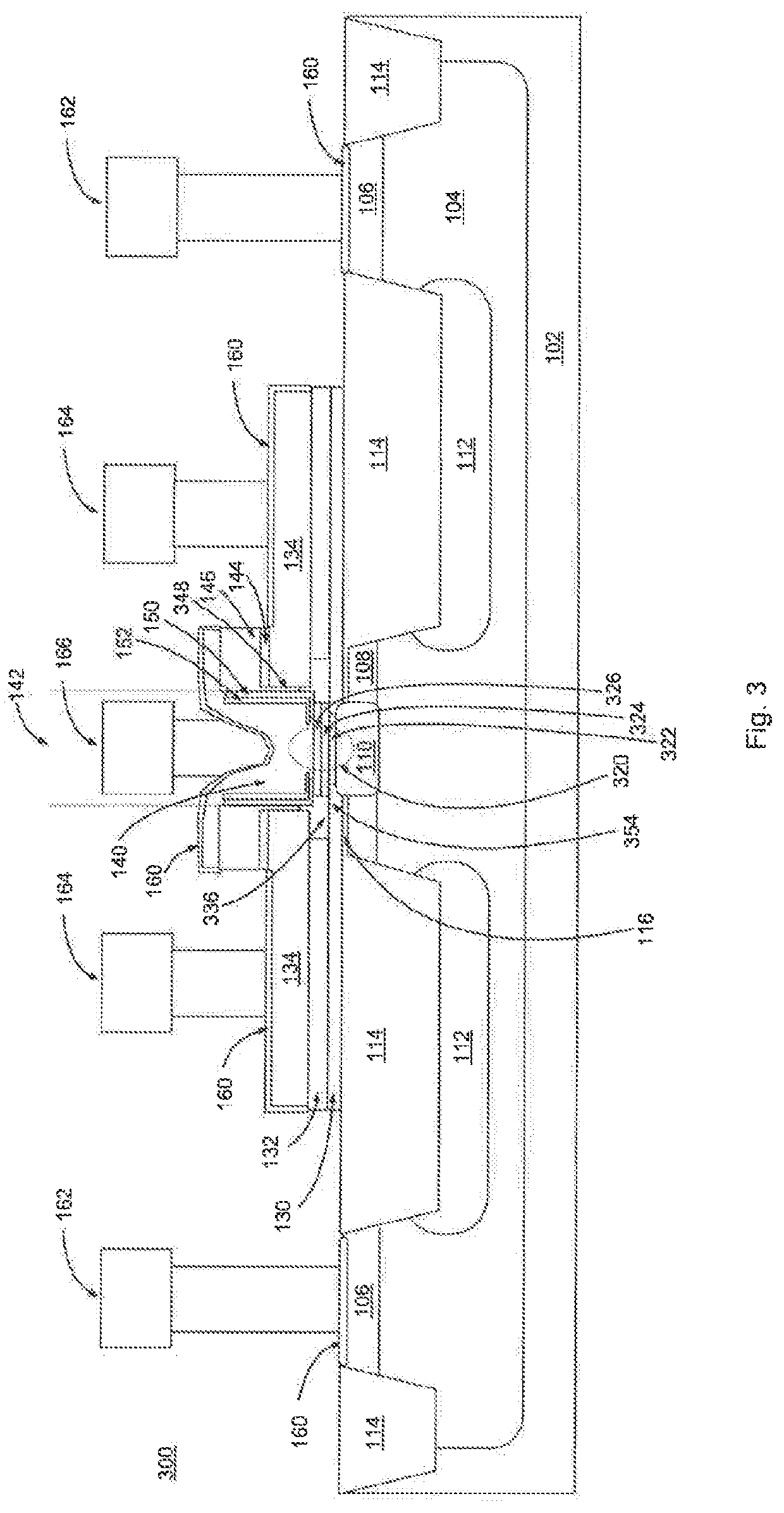
[0071]FIG. 3 shows a schematic cross-sectional view of a semiconductor device 300, in the form of a selective-epi base silicon germanium (SiGe) npn heterojunction bipolar transistor (HBT), according to the invention. Elements shown in FIG. 3 which correspond to elements described above with reference to FIGS. 1 and 2 are indicated by the same reference numbers. Semiconductor device 300 differs from semiconductor device 100 of FIG. 1 in that the base link region 336, which electrically couples the extrinsic base region 134 to the intrinsic base region 324, is grown from both the lower surface and the sidewall of the extrinsic base region 134.


PUM

PropertyMeasurementUnit
oscillation frequenciesaaaaaaaaaa
dielectricaaaaaaaaaa
etch ratesaaaaaaaaaa

Abstract

A semiconductor device comprises: an extrinsic base region; a first dielectric spacer on at least a part of a sidewall of the extrinsic base region adjacent to an emitter window region; an intrinsic base region; a base link region coupling the intrinsic base region and the extrinsic base region; a collector region underlying the intrinsic base region and having a periphery underlying the base link region; and a second dielectric spacer, separating the base link region from at least the periphery of the collector region; wherein said second dielectric spacer extends laterally beyond said first dielectric spacer to underlie said emitter window region.

Description

CROSS-REFERENCE TO RELATED APPLICATIONS[0001]This application claims the priority under 35 U.S.C. § 119 of European Patent application no. 18164437.8, filed on Mar. 27, 2018, the contents of which are incorporated by reference herein.FIELD OF THE INVENTION[0002]The present invention relates to a semiconductor device, and a method of manufacturing a semiconductor device, and relates particularly but not exclusively to a bipolar transistor and a method of manufacturing a bipolar transistor.BACKGROUND OF THE INVENTION[0003]In high-frequency applications, for example the 76 to 81 GHz band used for automotive radar, transistors with very high maximum oscillation frequencies are required. The two key parasitic device elements that limit the maximum oscillation frequency of a bipolar transistor are the base resistance and the collector-base capacitance. Device fabrication usually results in a trade-off between these two parasitic components. That is, higher-doped, deeper extrinsic base jun...

Claims


Application Information

Patent Timeline
Patent Type & Authority Patents(United States)
IPC IPC(8): H01L29/737H01L21/02H01L29/08H01L29/10H01L29/165H01L29/66H01L29/06
CPCH01L29/0653H01L29/66272H01L21/02532H01L29/66242H01L29/1004H01L21/02639H01L29/7371H01L29/0826H01L29/0817H01L29/165H01L29/0821H01L29/1008H01L29/737
Inventor JOHN, JAY PAULKIRCHGESSNER, JAMES
Owner NXP USA INC
Why Eureka
Try Eureka