Germanium-silicon heterogenous junction bipolar transistor and manufacturing method thereof

A technology of heterojunction bipolar and manufacturing methods, which is applied in the manufacture of germanium-silicon heterojunction bipolar transistors, and in the field of germanium-silicon heterojunction bipolar transistors, which can solve the problem that the outer base region cannot be made narrow and the maximum oscillation frequency is small. problem, to achieve the effect of reducing lateral diffusion, increasing the maximum oscillation frequency, and reducing width

Active Publication Date: 2013-06-05
SHANGHAI HUAHONG GRACE SEMICON MFG CORP
View PDF3 Cites 0 Cited by
  • Summary
  • Abstract
  • Description
  • Claims
  • Application Information

AI Technical Summary

Problems solved by technology

The technology of this device is mature and reliable, but the main disadvantages are: 1) The outer base region cannot be narrowed due to the external expansion of boron ions.
2) The maximum oscillation frequency (Fmax) is too small

Method used


Image

  • Germanium-silicon heterogenous junction bipolar transistor and manufacturing method thereof
  • Germanium-silicon heterogenous junction bipolar transistor and manufacturing method thereof
  • Germanium-silicon heterogenous junction bipolar transistor and manufacturing method thereof

Examples


Embodiment Construction

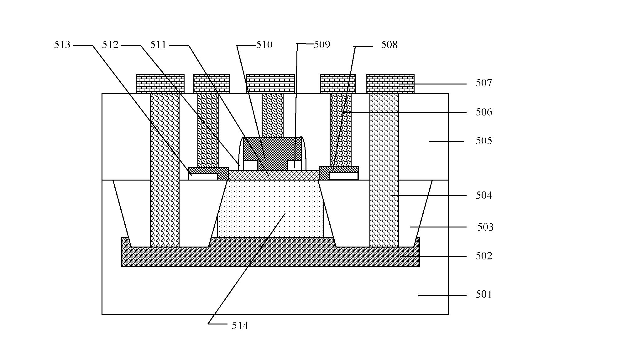
[0026] Such as figure 1 Shown is a schematic diagram of the device structure of a germanium-silicon heterojunction bipolar transistor according to an embodiment of the present invention. The germanium-silicon heterojunction bipolar transistor in the embodiment of the present invention is formed on the silicon substrate 501, and the active region is isolated by the shallow trench field oxygen 503, that is, the isolation structure of the active region is a shallow trench isolation. GeSi heterojunction bipolar transistors include:

[0027] A collector region 514 is composed of an N-type ion implantation region formed in the active region. The N-type ion implantation region of the collector region 514 can be formed by a single implant or multiple implants, the implanted impurity is arsenic or phosphorus, and the implanted energy and dose are determined by the silicon germanium heterojunction bipolar transistor The breakdown voltage is determined.

[0028] A pseudo-buried layer ...


PUM

PropertyMeasurementUnit
thicknessaaaaaaaaaa
thicknessaaaaaaaaaa
thicknessaaaaaaaaaa

Abstract

The invention discloses a germanium-silicon heterogenous junction bipolar transistor. An outer base region comprises germanium impurities or carbon impurities and P-type impurities, wherein the germanium impurities or the carbon impurities are injected in an autoregistration mode by using the outer side periphery of an emission region as an autoregistration boundary. The invention further discloses a manufacturing method of the germanium-silicon heterogenous junction bipolar transistor. According to the germanium-silicon heterogenous junction bipolar transistor and the manufacturing method of the germanium-silicon heterogenous junction bipolar transistor, due to the fact that the germanium impurities or the carbon impurities are injected into the outer base region, transverse diffusion of the P-type impurities can be reduced, the width of the outer base region can be reduced, and a maximum oscillation frequency of a device is improved.

Description

technical field [0001] The invention relates to the field of semiconductor integrated circuit manufacturing, in particular to a germanium-silicon heterojunction bipolar transistor; the invention also relates to a manufacturing method of the germanium-silicon heterojunction bipolar transistor. Background technique [0002] In radio frequency applications, higher and higher device characteristic frequencies are required. Although RFCMOS can achieve higher frequencies in advanced process technologies, it is still difficult to fully meet radio frequency requirements. For example, it is difficult to achieve characteristic frequencies above 40GHz, and advanced technology The research and development cost of compound semiconductors is also very high; compound semiconductors can realize very high characteristic frequency devices, but due to the disadvantages of high material cost and small size, and the toxicity of most compound semiconductors, its application is limited. Silicon ge...

Claims


Application Information

Patent Timeline
Patent Type & Authority Applications(China)
IPC IPC(8): H01L29/737H01L29/06H01L21/331H01L21/265
Inventor 陈帆陈雄斌薛恺周克然潘嘉李昊蔡莹陈曦
Owner SHANGHAI HUAHONG GRACE SEMICON MFG CORP
Why Eureka
Try Eureka