A kind of fabrication method of 4h-sic metal-semiconductor field-effect transistor with partially sunken channel
A field-effect transistor and metal-semiconductor technology, which is applied in the field of 4H-SiC metal-semiconductor field-effect transistors, can solve problems such as device breakdown voltage suppression and drop
- Summary
- Abstract
- Description
- Claims
- Application Information
AI Technical Summary
Problems solved by technology
Method used
Image
Examples
Embodiment 1
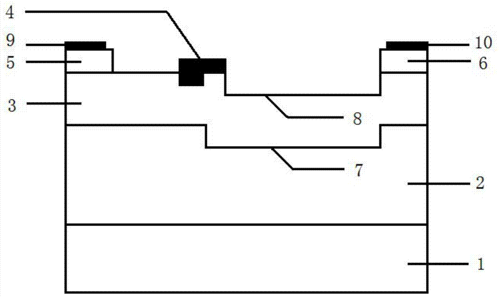
[0035] A 4H-SiC metal-semiconductor field-effect transistor with a recessed gate-drain buffer layer thickness and a recessed gate-drain drift region thickness of 0.1 μm is manufactured.
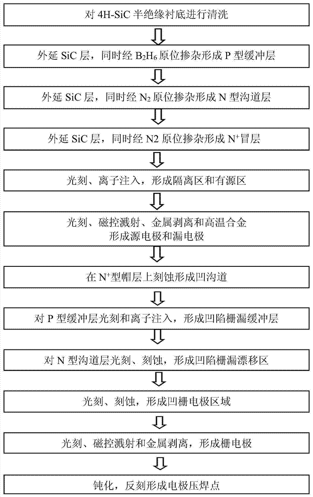
[0036] The manufacturing steps of this embodiment are as follows:
[0037] Step 1: cleaning the 4H-SiC semi-insulating substrate 1 to remove surface pollutants.
[0038] (1.1) Carefully wash the substrate twice with a cotton ball dipped in methanol to remove SiC particles of various sizes on the surface;
[0039] (1.2) Place the substrate in H 2 SO4 :HNO 3 = Ultrasound for 5 minutes in 1:1;
[0040] (1.3) Put the substrate in 1# cleaning solution (NaOH:H 2 o 2 :H 2 O=1:2:5), boiled for 5 minutes, rinsed with deionized water for 5 minutes, and then put into 2# cleaning solution (HCl:H 2 o 2 :H 2 O=1:2:7) and boiled for 5 minutes. Finally rinsed with deionized water and rinsed with N 2 Blow dry and set aside.
[0041] Step 2: epitaxially grow a SiC layer on the surface of the 4H-SiC...
Embodiment 2
[0085] A 4H-SiC metal-semiconductor field-effect transistor with a recessed gate-drain buffer layer thickness and a recessed gate-drain drift region thickness of 0.08 μm was fabricated.
[0086] Step 8: Photoetching and ion implanting the P-type buffer layer 2 to form a recessed gate-drain buffer layer 7 .
[0087] (8.1) Use positive photoresist, glue coating speed: 3000R / min, glue thickness > 2μm to ensure that it can play a good blocking role in the subsequent isolation injection;
[0088] (8.2) After gluing is completed, pre-bake in an oven at 90°C for 90 seconds, use a stepped buffer layer photolithography plate for about 35 seconds of UV exposure, and then develop in a special developer (tetramethylammonium hydroxide: water = 1:3) 60 seconds, then post-bake in an oven at 100°C for 3 minutes;
[0089] (8.3) Perform nitrogen ion implantation, the implantation condition is 240keV / 2×10 12 cm -2 , the temperature is 400°C. After the injection is completed, use acetone + ul...
Embodiment 3
[0097] A 4H-SiC metal-semiconductor field-effect transistor with a recessed gate-drain buffer layer thickness and a recessed gate-drain drift region thickness of 0.11 μm was fabricated.
[0098] Step 8: Photoetching and ion implanting the P-type buffer layer 2 to form a recessed gate-drain buffer layer 7 .
[0099] (8.1) Use positive photoresist, glue coating speed: 3000R / min, glue thickness > 2μm to ensure that it can play a good blocking role in the subsequent isolation injection;
[0100] (8.2) After gluing is completed, pre-bake in an oven at 90°C for 90 seconds, use a stepped buffer layer photolithography plate for about 35 seconds of UV exposure, and then develop in a special developer (tetramethylammonium hydroxide: water = 1:3) 60 seconds, then post-bake in an oven at 100°C for 3 minutes;
[0101] (8.3) Perform nitrogen ion implantation, the implantation condition is 270keV / 2×10 12 cm -2 , the temperature is 400°C. After the injection is completed, use acetone + ul...
PUM
 Abstract
Description
Claims
Application Information

