Semiconductor device and method of manufacturing the same

a technology of semiconductor devices and semiconductors, applied in the direction of semiconductor devices, electrical devices, transistors, etc., can solve the problems of insufficient mechanical strength, and achieve the effect of small base-collector junction capacity and high maximum oscillation frequency

Inactive Publication Date: 2007-10-02
RENESAS ELECTRONICS CORP
View PDF3 Cites 0 Cited by
  • Summary
  • Abstract
  • Description
  • Claims
  • Application Information

AI Technical Summary

Benefits of technology

[0009]The present invention allows a similar technological philosophy to be applied to a stacked semiconductor assembly, even in an emitter-up HBT. The collector layer in the E-up HBT is etched from the window section of an external base layer to reduce a base-collector junction capacity.
[0010]The present invention is characterized in that a base-emitter junction area smaller than a collector-base junction area can be formed by conducting a very small amount of side-etching without implanting an ion in a section adjacent to an intrinsic transistor section.
[0017]According to the present invention, it is possible to fabricate a semiconductor device having a C-up HBT small in base-collector junction capacity and high in maximum oscillation frequency.
[0018]According to the present invention, it is possible to fabricate a semiconductor device having a C-up HBT whose mechanical strength is ensured.
[0019]According to the present invention, it is possible to fabricate a semiconductor device having a C-up HBT free of area dependence on current gain.
[0020]According to the present invention, it is possible to fabricate a semiconductor device having a C-up HBT small in base-collector junction capacity.

Problems solved by technology

Accordingly, since a hollow region is formed directly under an external base layer, there has been the disadvantage of insufficient mechanical strength.

Method used


Image

  • Semiconductor device and method of manufacturing the same
  • Semiconductor device and method of manufacturing the same
  • Semiconductor device and method of manufacturing the same

Examples


first embodiment

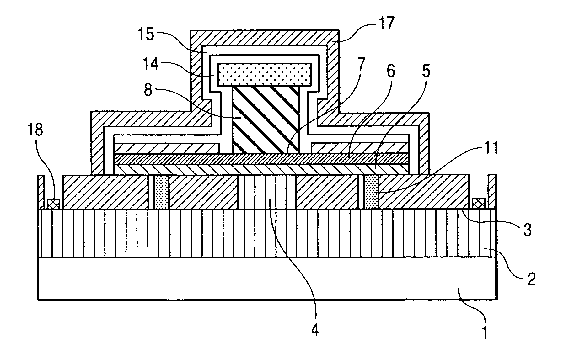
[0077]An npn-type C-up HBT, a first embodiment of the present invention, will be described using FIGS. 1 to 8C. In the present embodiment, as illustrated in longitudinal structural views of FIGS. 8B and 8C, a second emitter contact layer 4 is opened by etching from a window structure and by side-etching, and an effective emitter area of 0.5×0.5 μm2 (a contact area between the second emitter contact layer 4 and an emitter layer 5) is smaller than a base-collector area of 0.7×0.7 μm2 (a contact area between a base layer 6 and a collector layer 8). FIG. 8A is a top view of the C-up HBT, and FIGS. 8B, 8C are sectional views of an associated device, taken along lines 8B-8B, 8C-8C, respectively, in FIG. 8A.

[0078]A manufacturing process for the C-up HBT will be described below using FIGS. 1 to 8C.

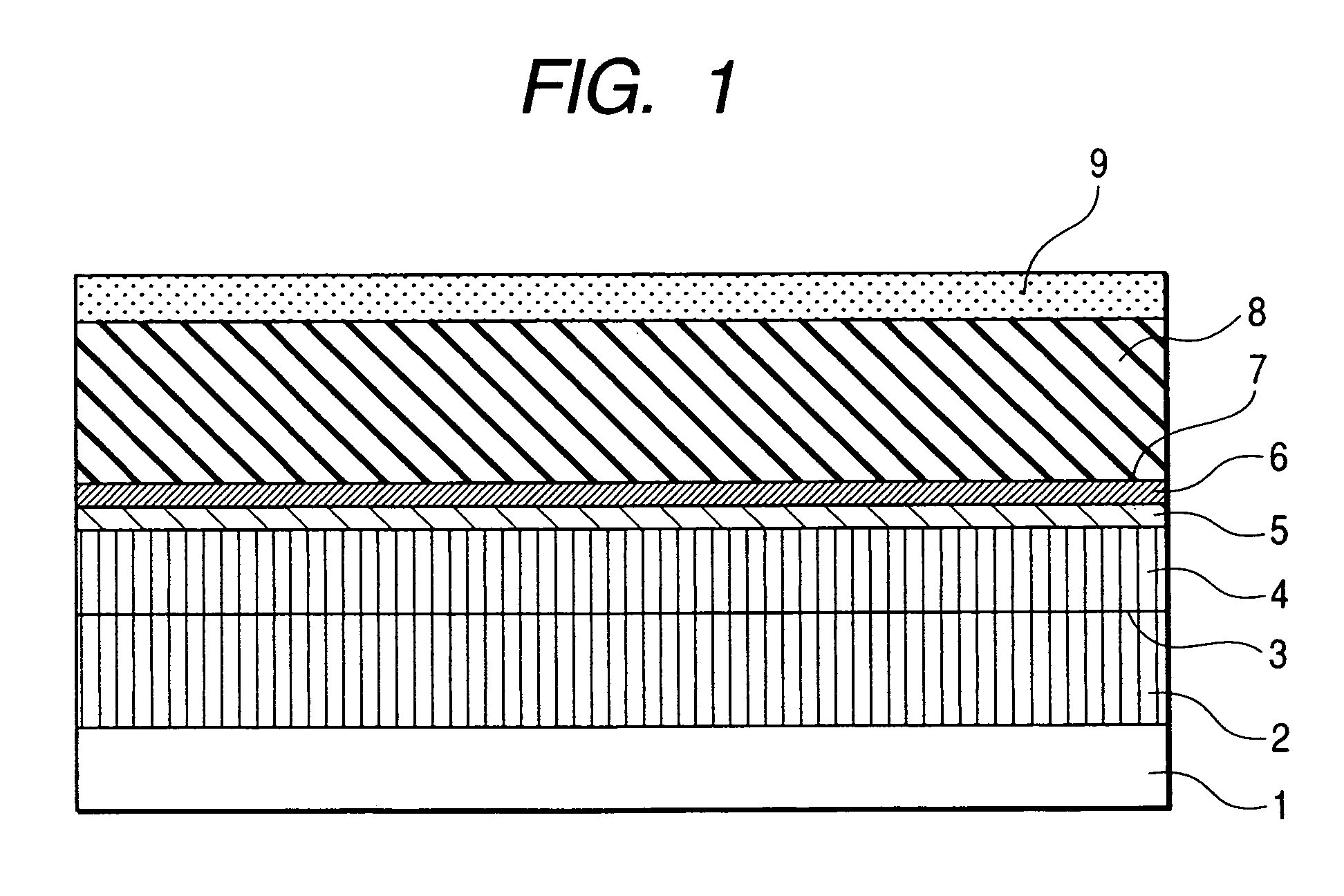
[0079]First, seven layers are formed on a semi-dielectric GaAs (100) substrate 1. That is to say, a first emitter contact layer 2, an etching stop layer 3, a second emitter contact layer 4, an n-t...

second embodiment

[0092]A second embodiment relates to a C-up HBT fabricated by forming an EB electrode after forming window structures, instead of forming an EB electrode before forming the window structures of the C-up HBT in the first embodiment. The present second embodiment will be described below using FIGS. 9 to 16C.

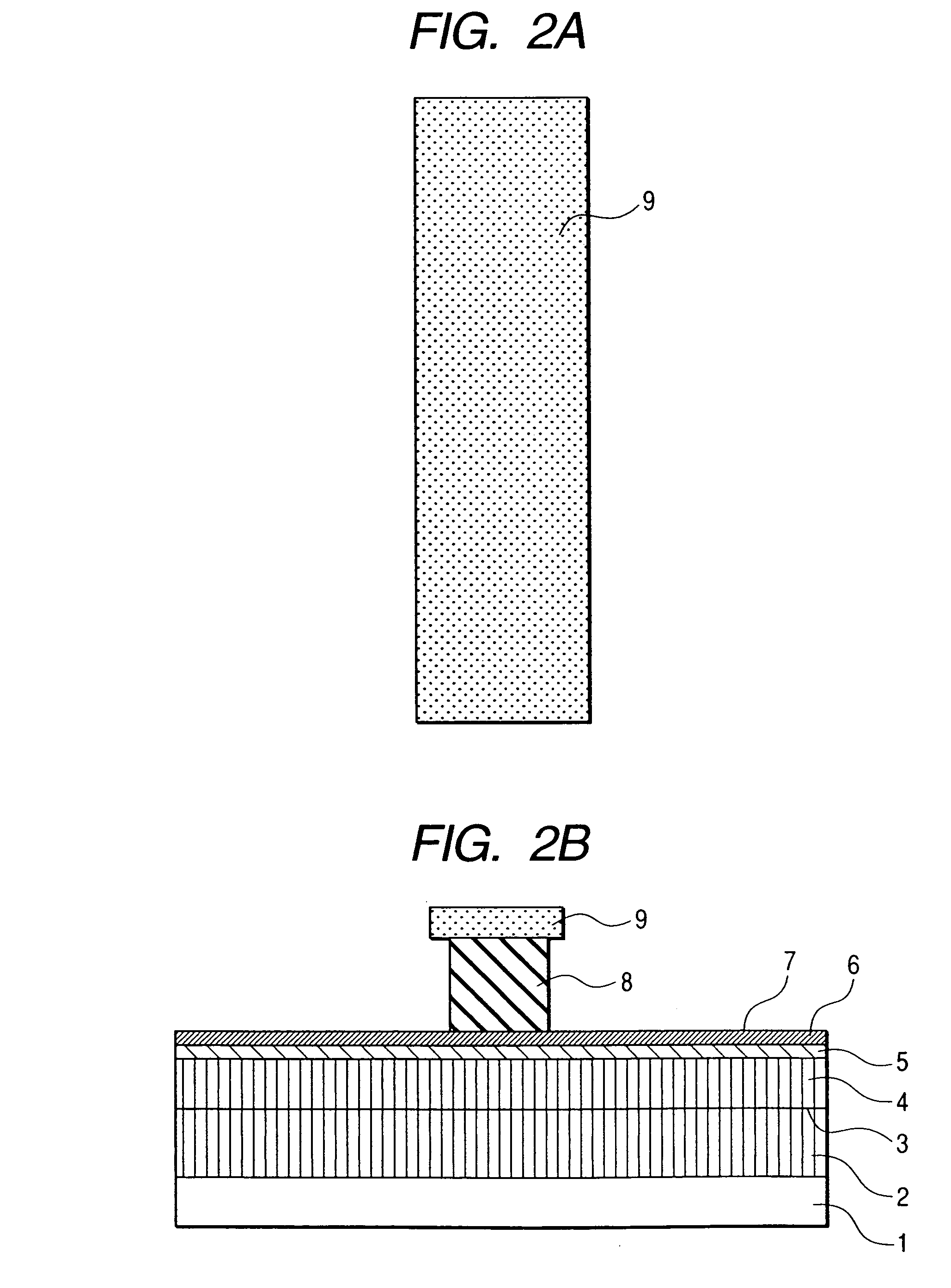
[0093]A layer structure similar / equivalent to that of the first embodiment is formed using metal-organic vapor phase epitaxy. The formation of the above layer structure is followed by depositing a WSi layer 9 (WSi: 0.3 in Si molar ratio, 0.5 μm in film thickness) on entire wafer surface using a high-frequency sputtering method (see FIG. 9). After that, dry etching with photolithography and CF4 is used to process the WSi layer into a desired shape and thus form a collector electrode 9. FIG. 10A shows a mask layout view, and FIG. 10B shows a longitudinal sectional view of the device formed in this process phase.

[0094]Next, dry etching with SF6 and SiCl4 and wet etching with a liquid ...

third embodiment

[0102]A third embodiment relates to an npn-type C-up HBT created by making changes as follows to the materials used in the first embodiment:

[0103](1) A semi-dielectric InP (100) substrate is used instead of the semi-dielectric GaAs (100) substrate 1.

[0104](2) An emitter contact layer made of highly doped InAlGaAs and having a 0.53 InAs molar ratio, a 5×1018cm−3 Si concentration, and a 0.5 μm film thickness, is formed instead of the first emitter contact layer 2 made of highly doped n-type GaAs.

[0105](3) An etching stop layer made of highly doped InAlGaAs and having a 0.5 InAs molar ratio, AlAs and GaAs molar ratios that are arbitrarily variable in progressive form, a 5×1017cm−3 Si concentration, and a 0.1 μm film thickness, is formed instead of the etching stop layer 3 made of highly doped n-type InGaP.

[0106](4) An emitter contact layer made of highly doped InGaAs and having a 0.5 InAs molar ratio, a 5×1018cm−3 Si concentration, and a 0.5 μm film thickness, is formed instead of the ...


PUM


Abstract

This invention is intended to provide an HBT capable of achieving, if the HBT is a collector-up HBT, the constriction of the emitter layer disposed directly under an external base layer, and reduction in base-emitter junction capacity, or if the HBT is an emitter-up HBT, reduction in base-collector junction capacity. For the collector-up HBT, window structures around the sidewalls of a collector are used to etch either the emitter layer disposed directly under the external base layer, or an emitter contact layer For the emitter-up HBT, window structures around the sidewalls of an emitter are used to etch either the collector layer disposed directly under the external base layer, or a collector contact layer. In both HBTs, the external base layer is supported by a columnar structure to ensure mechanical strength.

Description

CLAIM OF PRIORITY[0001]The present application claims priority from Japanese application JP 2004-380502 filed on Dec. 28, 2004, the content of which is hereby incorporated by reference into this application.BACKGROUND OF THE INVENTION[0002]The present invention relates to a semiconductor device with a heterojunction bipolar transistor which uses a compound semiconductor, and to a method of manufacturing the semiconductor device.[0003]Reduction in the emitter-base junction capacities and base-collector junction capacities of heterojunction bipolar transistors is closely associated with improvement of device performance characteristics such as an operating speed. In particular, collector-up heterojunction bipolar transistors (hereinafter, abbreviated to C-up HBTs), compared with emitter-up heterojunction bipolar transistors (hereinafter, abbreviated to E-up HBTs), have the advantages that the former can be reduced in parasitic collector capacity and enhanced in maximum oscillation fre...

Claims


Application Information

Patent Timeline
Patent Type & Authority Patents(United States)
IPC IPC(8): H01L31/109
CPCH01L29/7371H01L29/66318
Inventor TANAKA, KENICHITANOUE, TOMONORIMATSUMOTO, HIDETOSHIOHTA, HIROSHIMOCHIZUKI, KAZUHIROUCHIYAMA, HIROYUKI
Owner RENESAS ELECTRONICS CORP
Why Eureka
Try Eureka