Silicon-germanium heterojunction bipolar transistor and manufacturing method

A heterojunction bipolar transistor technology, applied in the manufacture of germanium-silicon heterojunction bipolar transistors, the field of germanium-silicon heterojunction bipolar transistors, can solve the problem of increasing the capacitance of the collector area, increasing the size, and unfavorable Ft Increase and other problems, to achieve the effect of low process cost

Active Publication Date: 2018-07-06
SHANGHAI HUAHONG GRACE SEMICON MFG CORP
View PDF4 Cites 0 Cited by
  • Summary
  • Abstract
  • Description
  • Claims
  • Application Information

AI Technical Summary

Problems solved by technology

The increased size of the local collector region 105 increases the c

Method used


Image

  • Silicon-germanium heterojunction bipolar transistor and manufacturing method
  • Silicon-germanium heterojunction bipolar transistor and manufacturing method
  • Silicon-germanium heterojunction bipolar transistor and manufacturing method

Examples


Embodiment Construction

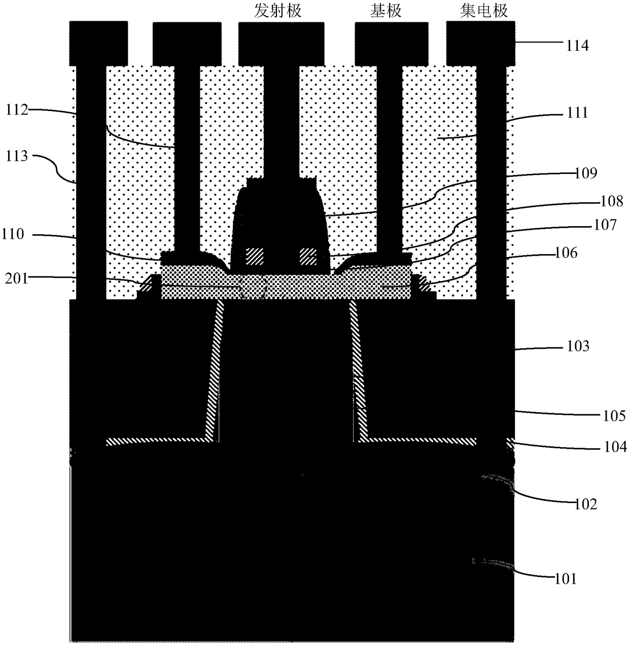
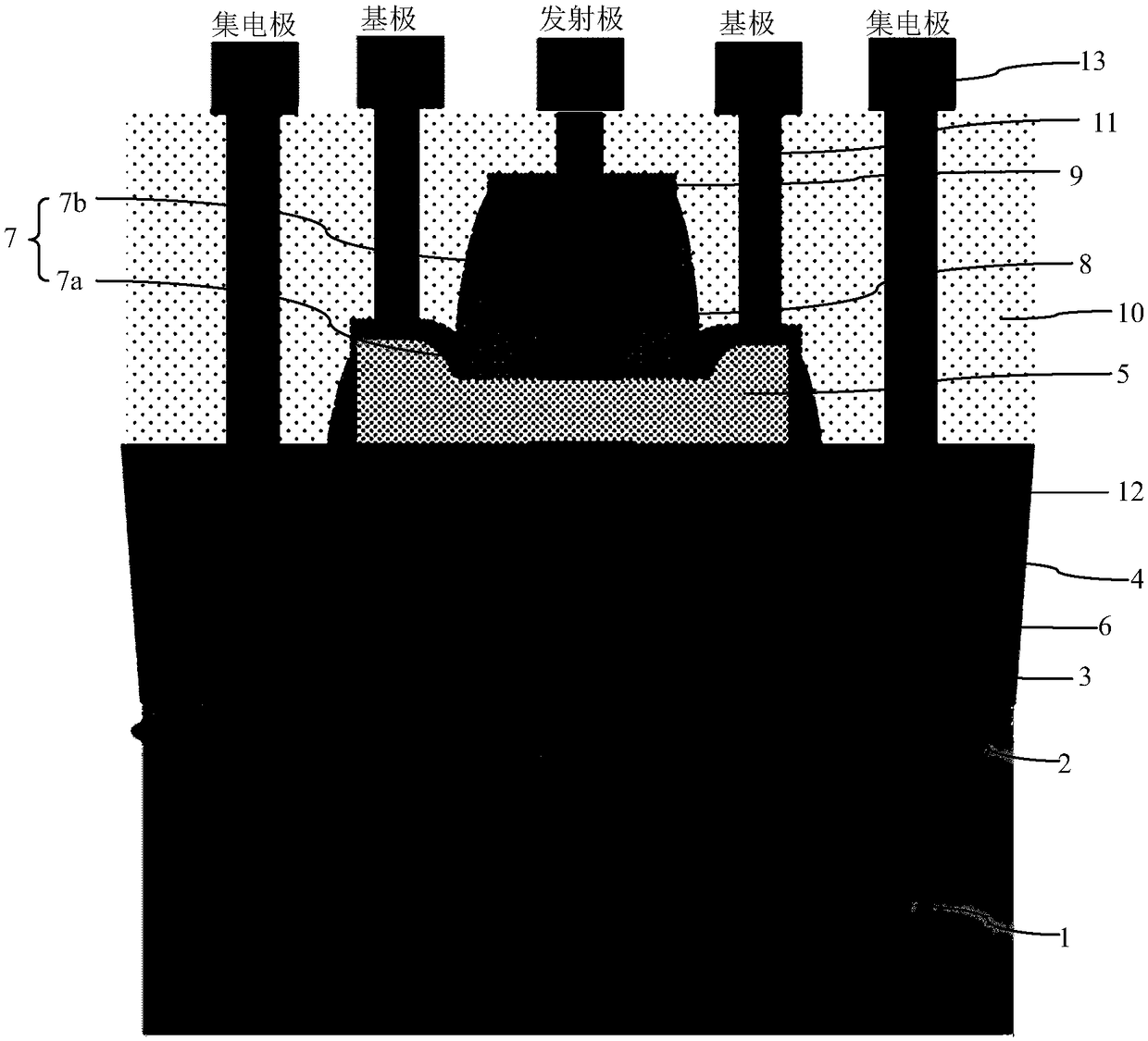
[0065] Such as figure 2 As shown, it is a schematic diagram of the structure of a silicon-germanium heterojunction bipolar transistor according to an embodiment of the present invention; , characterized in that the silicon-germanium heterojunction bipolar transistor comprises:

[0066] A collector region, including an overall collector region 3 and a partial collector region 6, the overall collector region 3 is composed of a first N-type ion implantation region formed in the entire active region; in the first N A second N-type ion implantation region is superimposed in a local area of ​​the N-type ion implantation region, and the local collector region 6 is formed by overlapping the second N-type ion implantation region and the first N-type ion implantation region.

[0067] The pseudo-buried layer 2 is composed of a heavily doped third N-type ion implantation region formed at the bottom of the field oxide layer 4 on both sides of the active region, the pseudo-buried layer 2 ...


PUM


Abstract

The invention discloses a silicon-germanium heterojunction bipolar transistor. A collector region consists of a global collector region and a local collector region, and is in contact with a pseudo buried layer. A base region is composed of a P-type silicon-germanium epitaxial layer formed on the surface of the collector region. An emitter region is composed of N-type polycrystalline silicon formed on the base region, and the N-type polycrystalline silicon consists of bottom polycrystalline silicon and top polycrystalline silicon. The local collector region and the emitter region window of thebottom polycrystalline silicon adopt the same photolithography definition to realize complete alignment of the local collector region and the bottom polycrystalline silicon. Before ion implantation in an outer base region, an emitter region window dielectric layer is removed. The ion implantation at a dip angle in the outer base region is self-aligned with the side of the bottom polycrystalline silicon, which increases the doping of an overlapping outer base region which is located outside the bottom polycrystalline silicon and covered by the top polycrystalline silicon and reduces the resistance of the base region. The invention further discloses a manufacturing method of the silicon-germanium heterojunction bipolar transistor. The characteristic frequency and the highest oscillation frequency of devices can be simultaneously improved. The silicon-germanium heterojunction bipolar transistor is applicable to the ultrahigh-frequency application requirement of devices, and is of low process cost.

Description

technical field [0001] The invention relates to the field of semiconductor integrated circuit manufacturing, in particular to a silicon-germanium (SiGe) heterojunction bipolar transistor (HBT); the invention also relates to a method for manufacturing the silicon-germanium heterojunction bipolar transistor. Background technique [0002] UHF RF applications require improved characteristic frequency (F t ) and the highest oscillation frequency (F max ). The characteristic frequency is also called the cut-off frequency, which is the frequency when the current gain is 1; the highest oscillation frequency is the frequency when the power gain is 1. [0003] The fully self-aligned SiGe HBT manufacturing process can obtain a very high characteristic frequency and the highest oscillation frequency, but the manufacturing process is complex and requires a selective SiGe epitaxial process. [0004] Such as figure 1 Shown is a schematic diagram of the existing germanium-silicon hetero...

Claims


Application Information

Patent Timeline
IPC IPC(8): H01L29/737H01L21/331
CPCH01L29/66242H01L29/7378
Inventor 钱文生
Owner SHANGHAI HUAHONG GRACE SEMICON MFG CORP
Why Eureka
Try Eureka