Semiconductor structure and method for forming the same

a technology soi structure, which is applied in the direction basic electric elements, electrical appliances, etc., can solve the problem of increasing off-state leakage current, low heat conductivity of siosub>2 /sub>insulating layer in soi structure, and reducing parasitic junction capacitance of source and drain, inhibiting band-to-band

Inactive Publication Date: 2013-11-19
TSINGHUA UNIV
View PDF3 Cites 0 Cited by
  • Summary
  • Abstract
  • Description
  • Claims
  • Application Information

AI Technical Summary

Benefits of technology

[0027]According to an embodiment of the present disclosure, the floated films are used as a source region and a drain region respectively. In this way, on one hand, dopants in the source and the drain maybe prevented from diffusing into a substrate, so that an ultra-shallow junction may be easy to fabricate. On the other hand, the source and the drain may not contact with the substrate, thus inhibiting band-to-band tunneling (BTBT) leakage between the source and the substrate and between the drain and the substrate. Furthermore, parasitic junction capacitance of the source and the drain may be reduced, thus improving the performance of the device. Moreover, with the semiconductor structure according to an embodiment of the present disclosure, the floated films, for example, a Si layer, a SiyGe1-y layer, a Ge layer, or an III-V group compound semiconductor layer, may be formed, thus improving the performance of the device.
[0028]Conventionally, if a SOI structure is used, a heat dissipation of a channel may be hindered by an insulating layer. However, with the semiconductor structure according to an embodiment of the present disclosure, by using the convex structures as a channel, a problem of inhibiting the heat dissipation of the channel by the insulating layer in the SOI structure may be effectively alleviated, and a leakage of the device may be reduced like the SOI structure, thus improving the performance of the device.

Problems solved by technology

However, a serious challenge is an emergence of a short-channel effect, such as a subthreshold voltage roll-off (Vt roll-off), a DIBL (drain-induced barrier lowering) and a source-drain punch through, thus increasing an off-state leakage current.
Therefore, a performance of the MOSFET may be deteriorated.
In addition, a leakage may be alleviated by a SOI (silicon on insulator) structure, however, a heat conductivity of a SiO2 insulating layer in the SOI structure is low, so that a heat generated in a channel in a small size device may be difficult to dissipate.
Therefore, for a conventional device, large leakage and difficult heat dissipation are main constraints for scaling down.

Method used


Image

  • Semiconductor structure and method for forming the same
  • Semiconductor structure and method for forming the same
  • Semiconductor structure and method for forming the same

Examples


Embodiment Construction

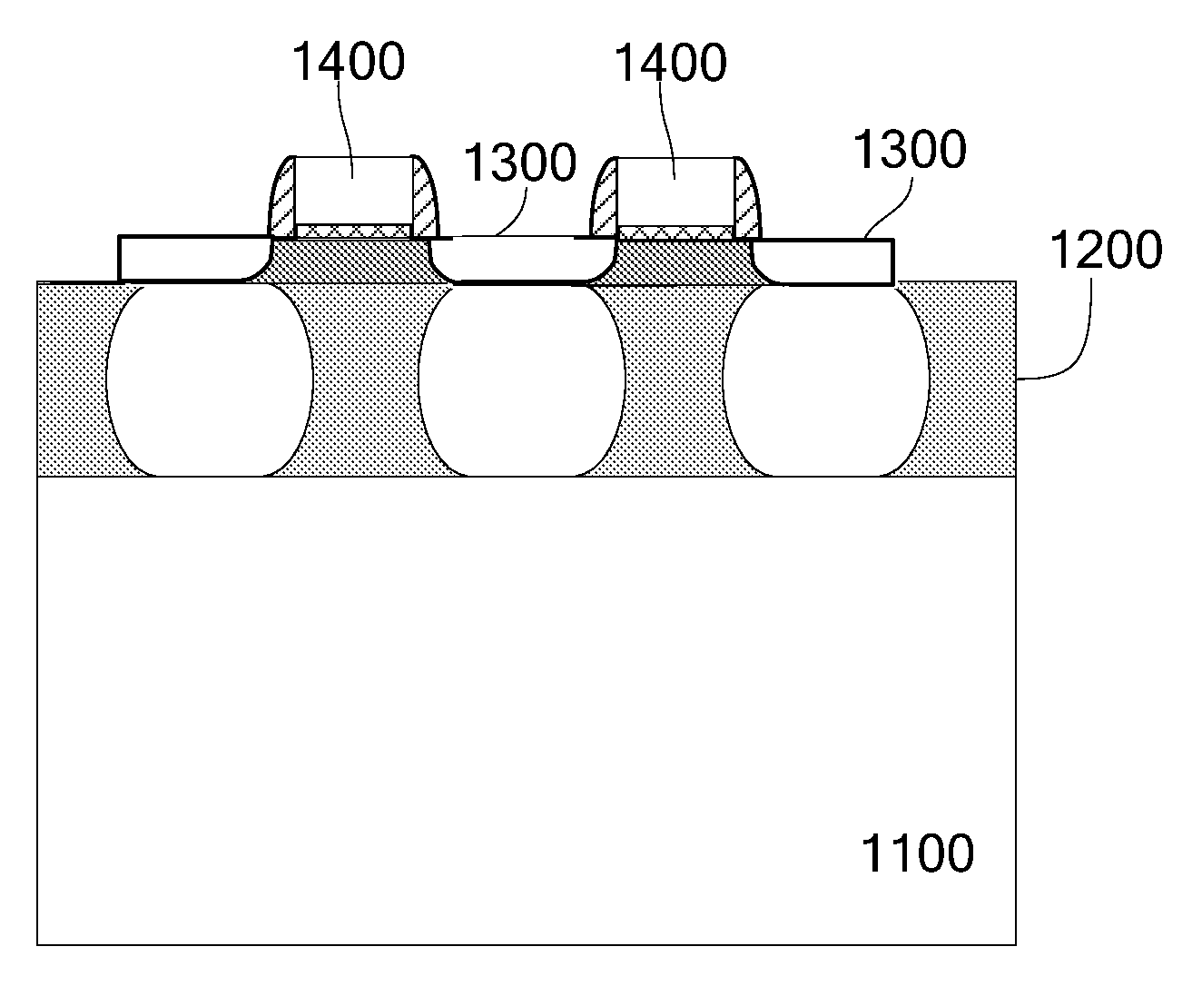
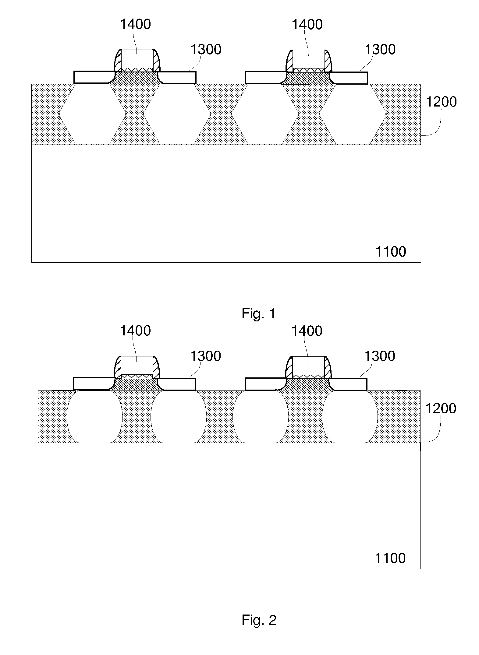
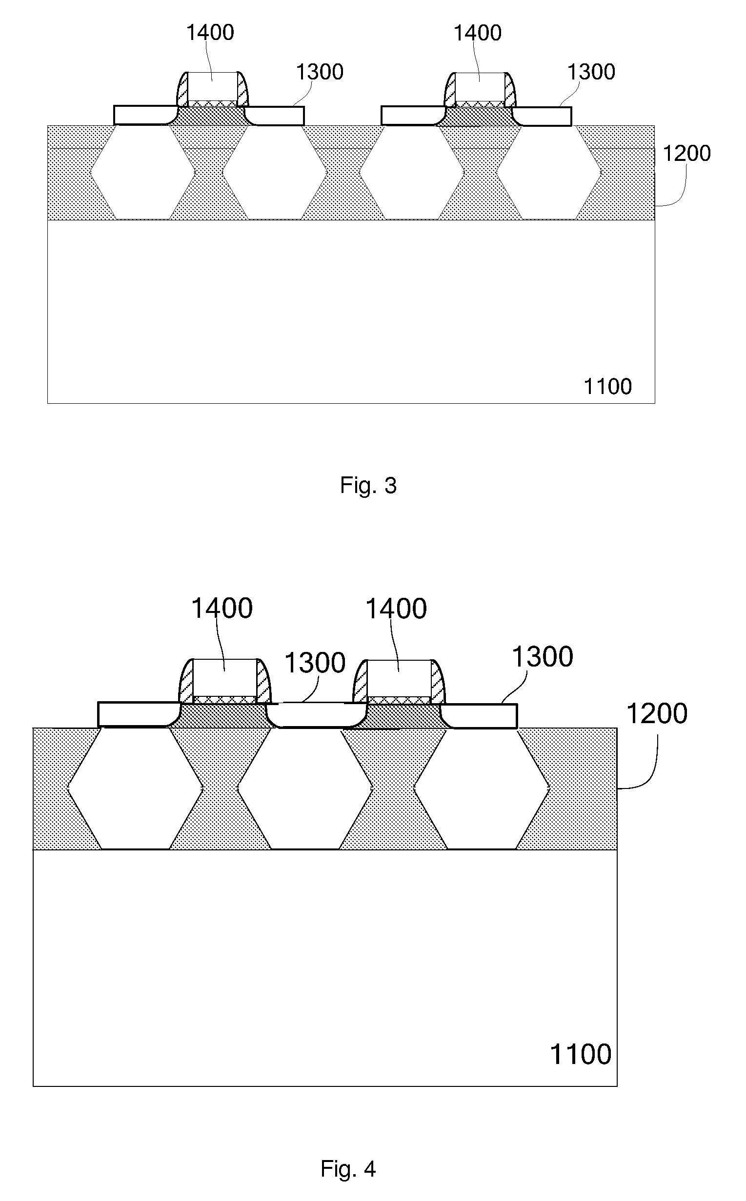
[0037]Embodiments of the present disclosure will be described in detail in the following descriptions, examples of which are shown in the accompanying drawings, in which the same or similar elements and elements having same or similar functions are denoted by like reference numerals throughout the descriptions. The embodiments described herein with reference to the accompanying drawings are explanatory and illustrative, which are used to generally understand the present disclosure. The embodiments shall not be construed to limit the present disclosure.

[0038]Various embodiments and examples are provided in the following description to implement different structures of the present disclosure. In order to simplify the present disclosure, certain elements and settings will be described. However, these elements and settings are only examples and are not intended to limit the present disclosure. In addition, reference numerals may be repeated in different examples in the disclosure. This ...


PUM


Abstract

A semiconductor structure and a method for forming the same are provided. The semiconductor structure includes a substrate; a plurality of convex structures formed on the substrate, in which every two adjacent convex structures are separated by a cavity; a plurality of floated films, in which each floated film is formed between the every two adjacent convex structures and connected with tops of the every two adjacent convex structures, the floated films are partitioned into a plurality of sets, a channel layer is formed on a convex structure between the floated films in each set, a source region and a drain region are formed on two sides of the channel layer respectively, and an isolation portion is set between two adjacent sets of floated films; and a gate stack formed on each channel layer.

Description

CROSS-REFERENCE TO RELATED PATENT APPLICATIONS[0001]The present application is a national phase entry under 35U.S.C. §371 of International Application No. PCT / CN2011 / 082110 filed Nov. 11, 2011, published in English, which claims priority from Chinese Application No. 201110149714.5, filed Jun. 3, 2011, all of which are incorporated herein by reference.FIELD OF THE INVENTION[0002]The present disclosure relates to a semiconductor manufacture and design, and more particularly to a semiconductor structure and a method for forming the same.BACKGROUND OF THE INVENTION[0003]For a long time, in order to achieve a higher chip density, a faster working speed and a lower power consumption, a feature size of a MOSFET (metal-oxide-semiconductor field effect transistor) is continuously scaled down according to Moore's law, and a working speed of the MOSFET is faster and faster. Currently, the feature size of the MOSFET has reached a nanometer level. However, a serious challenge is an emergence of ...

Claims


Application Information

Patent Timeline
Patent Type & Authority Patents(United States)
IPC IPC(8): H01L29/78
CPCH01L21/764H01L21/823412H01L21/823418H01L21/823481
Inventor WANG, JINGGUO, LEI
Owner TSINGHUA UNIV
Why Eureka
Try Eureka