Optical element and light irradiation apparatus

a technology of optical elements and light irradiation apparatus, which is applied in the direction of photomechanical apparatus, instruments, record information storage, etc., can solve the problems of inability to completely uniformly uniformly curvature or profile irregularities of each cylindrical lens, and the melting point is lower than a synthesized quartz substrate, so as to improve the homogeneity of laser beam intensity.

Inactive Publication Date: 2008-10-07
SEMICON ENERGY LAB CO LTD +1
View PDF16 Cites 7 Cited by
  • Summary
  • Abstract
  • Description
  • Claims
  • Application Information

AI Technical Summary

Benefits of technology

[0012]In view of the foregoing problems, it is an object of the present invention to provide technique which can improve homogeneity of intensity of a laser beam and homogenize energy distribution of a beam spot on an irradiated surface. Moreover, it is another object of the invention to provide technique which can form a beam spot with homogeneous energy distribution and a desired size on an irradiated surface.
[0013]Further, it is another object of the invention to provide technique which can optimize the size of a beam spot in accordance with an object to be irradiated and form a beam spot having a similar figure.
[0014]It is another object of the invention to provide technique which can improve homogeneity of intensity of a beam emitted from a light source such as a xenon lamp, a halogen lamp, or a high pressure mercury lamp, which is not limited to a laser beam, and homogenize energy distribution of a beam spot on an irradiated surface.

Problems solved by technology

The glass substrate has an advantage that an inexpensive and large-sized substrate can be easily manufactured compared with a synthesized quartz substrate, but also has a disadvantage that a melting point is lower than a synthesized quartz substrate.
However, in the case of using a cylindrical lens array, processing precision of individual cylindrical lens becomes a problem.
A cylindrical lens array is a line of a plurality of cylindrical lenses; however, it is impossible to completely uniform a radius of curvature or profile irregularity of each cylindrical lens.
This can be a problem in conducting laser annealing to a semiconductor film.
Further, a conventional light irradiation apparatus does not have a structure which can form a beam spot with a desired size in accordance with the size of a region to be irradiated.

Method used


Image

  • Optical element and light irradiation apparatus
  • Optical element and light irradiation apparatus
  • Optical element and light irradiation apparatus

Examples


embodiment mode 1

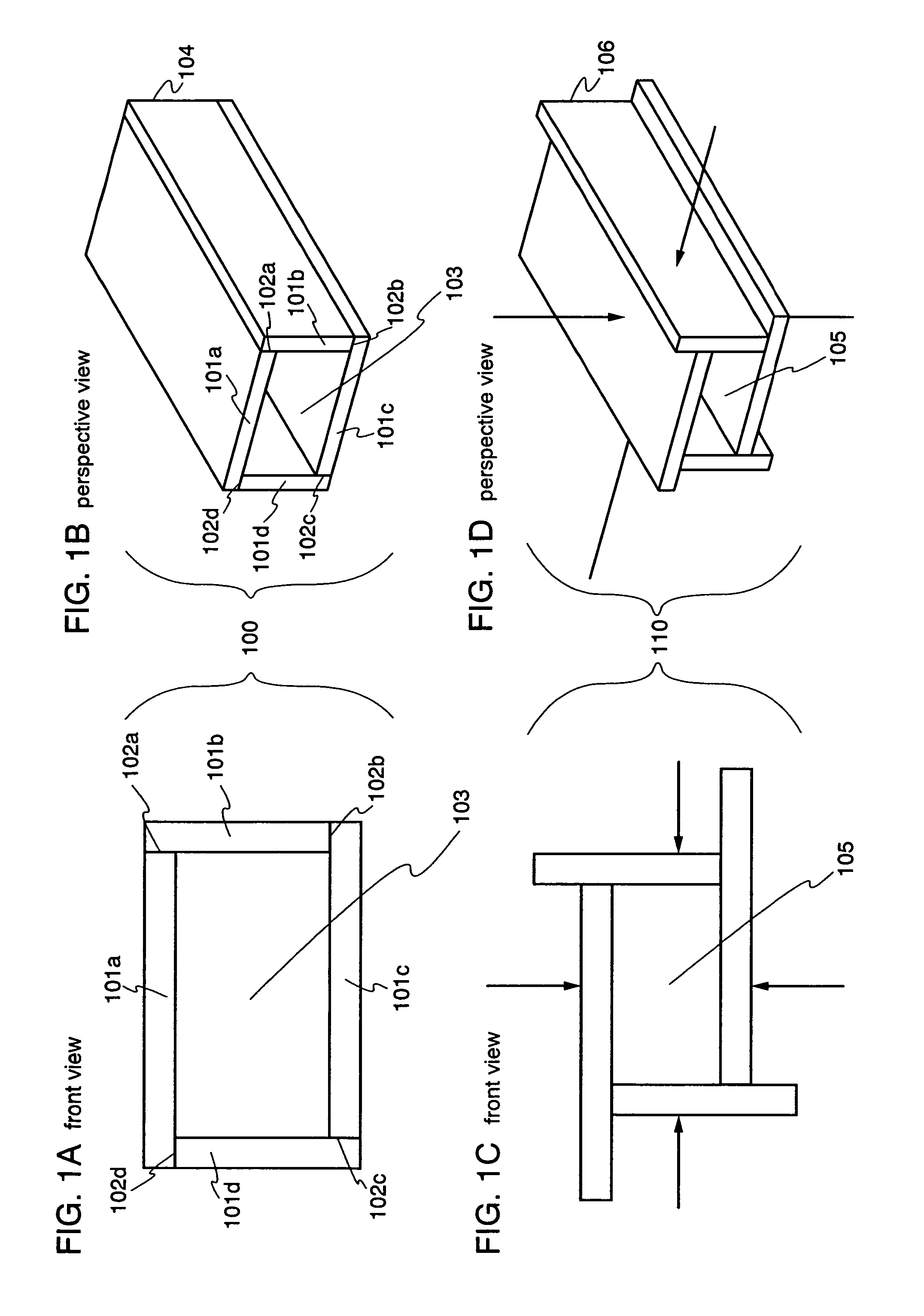
[0064]The present invention relates to an optical element which homogenizes energy distribution of a beam spot on an irradiated surface. Hereinafter, an optical element according to the invention will be specifically explained with reference to FIGS. 1A to 1D.

[0065]The optical element disclosed in the invention has a plurality of reflectors to form a polygonal entrance and exit. It is to be noted that the shapes of the entrance and the exit according to the invention are the same. The intensity distribution of a beam which is entered the optical element is homogenized in the optical element, then, the beam reaches an irradiated surface, which forms a beam spot with homogeneous energy distribution on the irradiated surface. At this time, the shape of the entrance and the exit of the optical element becomes a shape of the beam spot on the irradiated surface.

[0066]In accordance with the optical element disclosed in the invention, the size or shape of the entrance and the exit can be ch...

embodiment mode 2

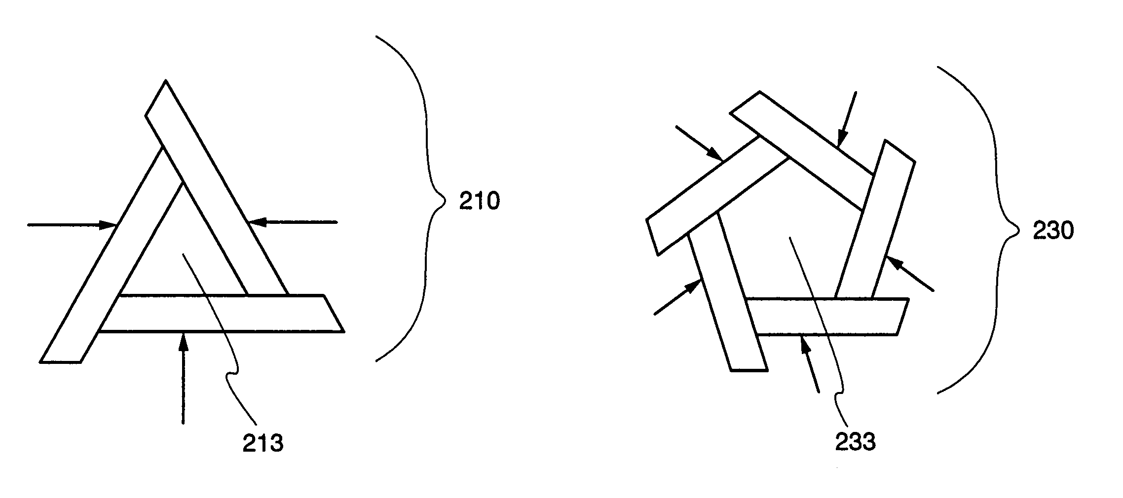
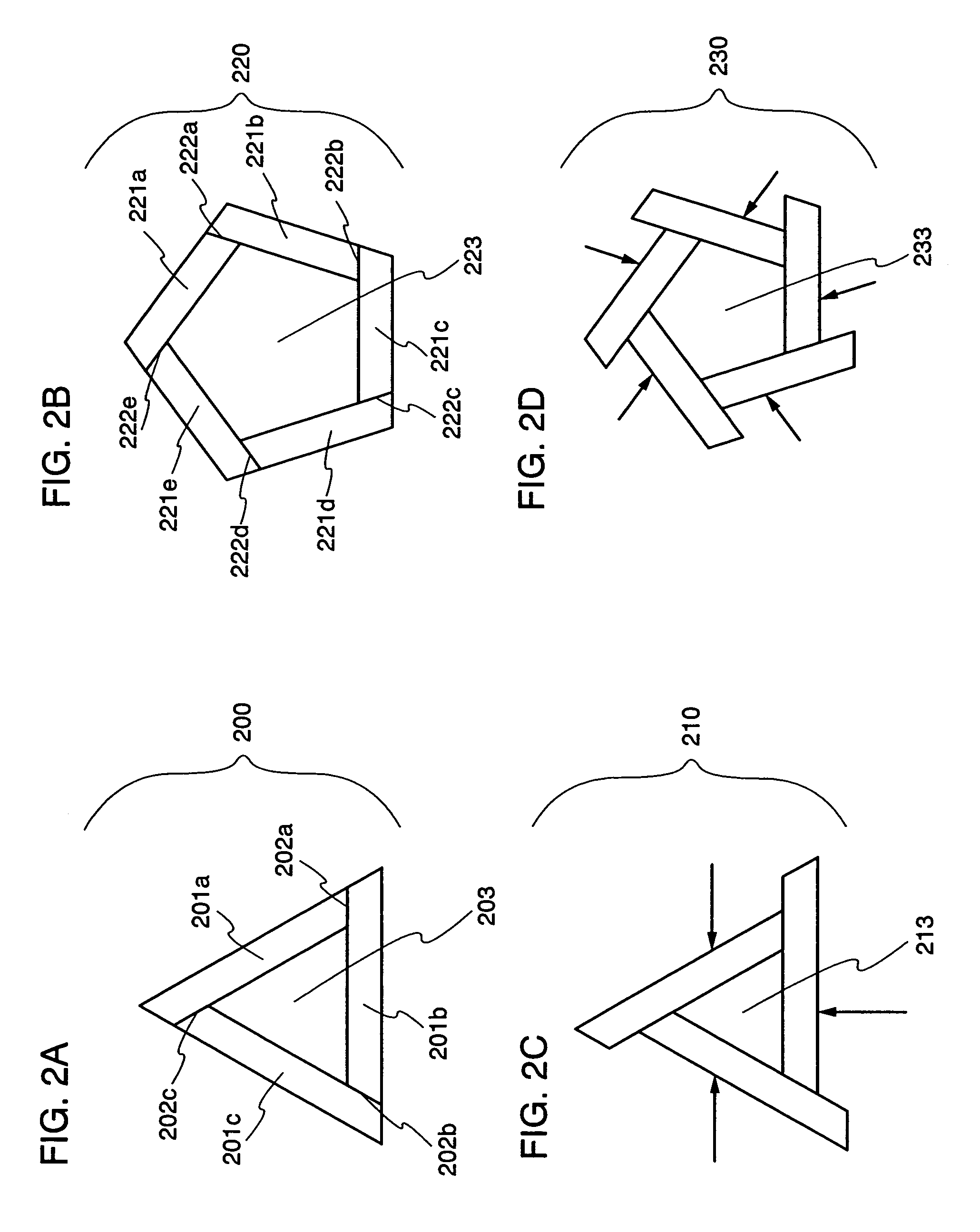
[0076]In this embodiment mode, an optical element in which the shape of an entrance is different from that in Embodiment Mode 1 will be explained with reference to FIGS. 2A to 2D. FIGS. 2A to 2D are front views of the optical element which will be explained in this embodiment mode.

[0077]FIG. 2A is an optical element 200 having a triangular entrance 203, and FIG. 2B is an optical element 220 having a pentagonal entrance 223. Each optical element has a plurality of reflectors for forming a polygonal entrance and exit in the same manner as the optical element described in Embodiment Mode 1. It is to be noted that the shape of the exit is the same as the shape of the entrance in the same manner as Embodiment Mode 1. In FIG. 2A, the optical element 200 has three reflectors 201a to 201c for forming the triangular entrance 203 of the optical element 200, and in FIG. 2B, the optical element 220 has five reflectors 221a to 221e for forming the pentagonal entrance 223 of the optical element 2...

embodiment mode 3

[0083]In this embodiment mode, an optical system of a light irradiation apparatus will be explained, in which a light source, an optical element disclosed in the present invention described above, and a convex spherical lens between the light source and the optical element and between the optical element and an irradiated surface, respectively, are arranged.

[0084]In FIGS. 3A and 3B, a beam propagates in a direction indicated by an arrow. In FIGS. 3A and 3B, the beam emitted from a light source 301 is converged by a convex spherical lens 302. In this embodiment mode, a laser oscillator is used as the light source; however, in addition to this, a xenon lamp, a halogen lamp, a high pressure mercury lamp, or the like can be used. In the case where the xenon lamp, the halogen lamp, and the high pressure mercury lamp are used as the light source, an elliptical mirror is preferably arranged in the opposite side of the irradiated surface with respect to the light source because a beam emitt...


PUM


Abstract

It is an object of the present invention to provide an optical element which forms a beam spot with homogeneous energy distribution on an irradiated surface, and a light irradiation apparatus. It is another object of the invention to provide a manufacturing method of a semiconductor device using a beam spot with homogeneous energy distribution. One feature of the invention is to homogenize energy distribution of a beam spot on an irradiated surface by forming the optical element provided with a polygonal entrance and exit using a plurality of reflectors as side walls and introducing a beam to the optical element. Further, a beam spot with a desired size or shape can be obtained by making the reflectors movable. Furthermore, by using a light irradiation apparatus using the optical element, failure in manufacturing a semiconductor device can be reduced.

Description

BACKGROUND OF THE INVENTION[0001]1. Field of the Invention[0002]The present invention relates to an optical element which homogenizes energy distribution of a beam spot on an irradiated surface in a specific region, and a light irradiation apparatus using the optical element. Moreover, the invention relates to a manufacturing method of a semiconductor device in which a crystalline semiconductor film formed using the light irradiation apparatus is used.[0003]2. Description of the Related Art[0004]In recent years, technique for manufacturing a thin film transistor (hereinafter, referred to as a TFT) over a substrate has been drastically advanced, and the application and development thereof to an active matrix display device has been promoted. In particular, a TFT in which a polycrystalline semiconductor film is used has higher electron field-effect mobility (also referred to as mobility) than a conventional TFT in which a non-single crystal semiconductor film is used; therefore, high ...

Claims


Application Information

Patent Timeline
Patent Type & Authority Patents(United States)
IPC IPC(8): G02B6/00
CPCG03F7/70075
Inventor TANAKA, KOICHIRO
Owner SEMICON ENERGY LAB CO LTD
Why Eureka
Try Eureka