Solid state imaging apparatus, method for driving the same and camera using the same

a technology of solid-state imaging and camera, which is applied in the direction of television system scanning details, radioation control devices, television systems, etc., can solve the problems of reducing the size of the photoelectric conversion cell, unable to ensure a sufficiently large opening area of the pd section b>101, etc., and achieves high-resolution images

Active Publication Date: 2008-10-14
GK BRIDGE 1
View PDF25 Cites 19 Cited by
  • Summary
  • Abstract
  • Description
  • Claims
  • Application Information

AI Technical Summary

Benefits of technology

[0040]A camera according to the present invention includes the first or second solid state imaging apparatus of the present invention. Thus, the camera of the present invention can achieve a high resolution image.

Problems solved by technology

For example, if a photoelectric conversion cell is designed, assuming that the area of a photoelectric conversion cell is 4.1 μm×4.1 μm, with the design rule of 0.35 μm, the aperture ratio of the PD section 101 to the photoelectric conversion cell is only about 5% Therefore, it is difficult to ensure a sufficiently large area of opening of the PD section 101 and also to reduce the size of the photoelectric conversion cell.

Method used


Image

  • Solid state imaging apparatus, method for driving the same and camera using the same
  • Solid state imaging apparatus, method for driving the same and camera using the same
  • Solid state imaging apparatus, method for driving the same and camera using the same

Examples


first embodiment

Modified Example of First Embodiment

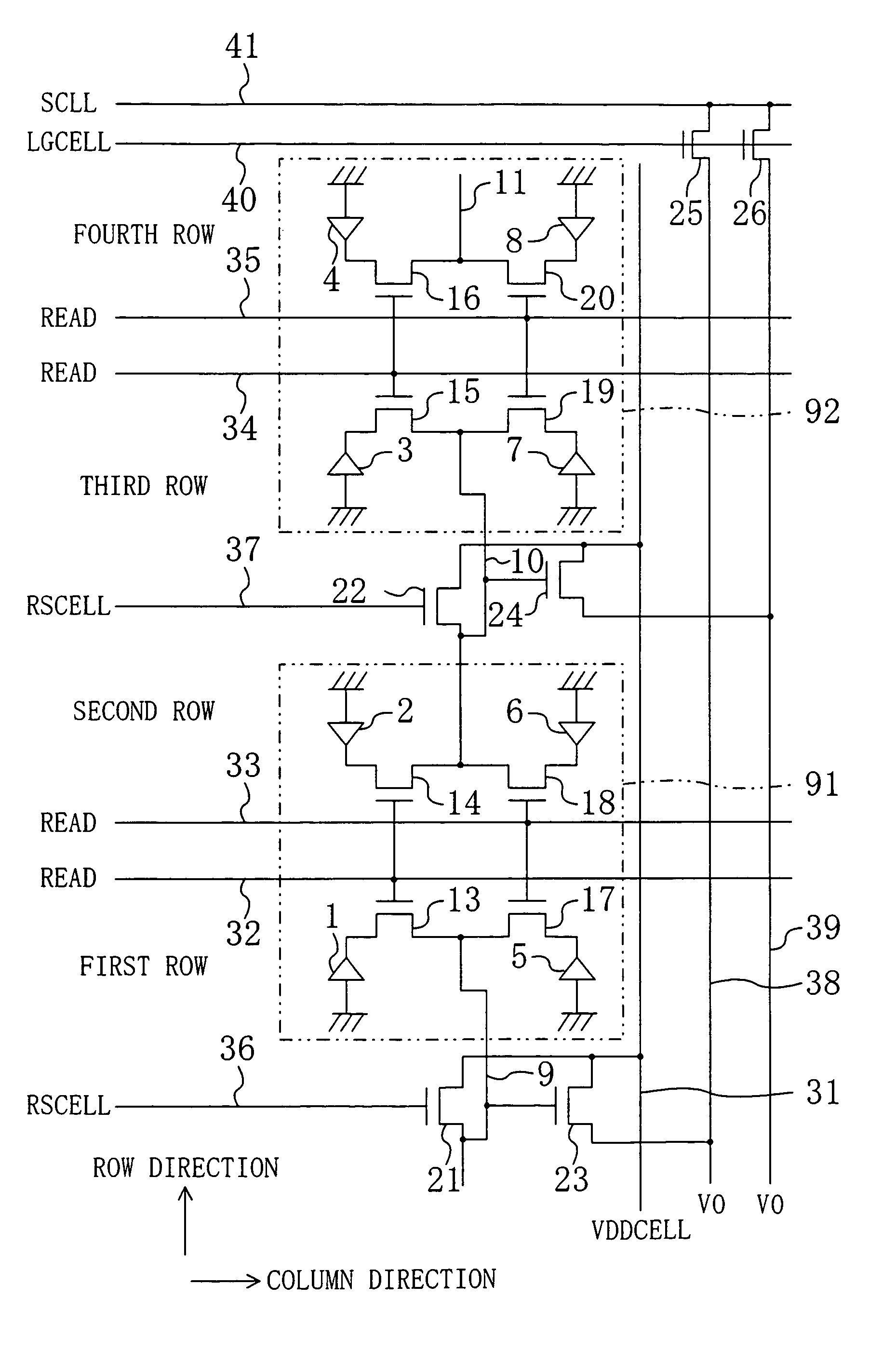
[0084]FIG. 3 is a diagram illustrating a circuit configuration of a photoelectric conversion cell in a solid state imaging apparatus according to a modified example of the first embodiment of the present invention. Also, in this modified example each member also shown in FIG. 1 is identified by the same reference numeral, and therefore, description thereof will be omitted.

[0085]As shown in FIG. 3, for example, in the first photoelectric conversion cell 91, the first READ line 32 is connected to the transfer transistor 13 and the transfer transistor 18 included in adjacent columns, respectively, while the second READ line 33 is connected to the transfer transistor 14 and the transfer transistor 17 included in adjacent columns, respectively. Thus, even if connections are made with respect to the PD sections 1, 2, 5 and 6 included in two adjacent rows with the first and second READ lines 32 and 33 interposed between the PD sections 1 and 5 and the PD...

second embodiment

[0089]Hereinafter, a second embodiment of the present invention will be described with reference to the accompanying drawings.

[0090]FIG. 4 is a diagram illustrating an example of circuit configuration of a photoelectric conversion cell in a solid state imaging apparatus according to a second embodiment of the present invention. In FIG. 4, each member also shown in FIG. 1 is identified by the same reference numeral, and therefore, description thereof will be omitted.

[0091]First, differences of the solid state imaging apparatus of FIG. 4 from that of the first embodiment shown in FIG. 1 will be described.

[0092]In the second embodiment, an configuration in which the first and second pixel amplifier transistors 23 and 24 are connected to the first and second output signal (VO) lines 38 and 39, respectively, via the first and second select transistors 52 and 53 each of which made of an N channel FET, respectively, is used.

[0093]To the respective gates of the first and second select trans...

third embodiment

[0107]Hereinafter, a third embodiment of the present invention will be described with reference to the accompanying drawings.

[0108]FIG. 6 is a diagram illustrating an example of circuit configuration of a photoelectric conversion cell in a solid state imaging apparatus according to a third embodiment of the present invention. In FIG. 6, each member also shown in FIG. 1 is identified by the same reference numeral, and therefore, description thereof will be omitted.

[0109]As shown in FIG. 6, in the solid state imaging apparatus of the third embodiment, first through fourth photoelectric conversion cells 91, 92, 93 and 94 are arranged in a matrix.

[0110]For example, the first photoelectric conversion cell 91 includes photoelectric conversion (PD) sections 1 and 2 arranged in regions which is located in the first column of an array and the first row and which is located in the first column of and the second rows of the array, respectively. The PD sections 1 and 2 share a first FD section ...


PUM


Abstract

A solid state imaging apparatus includes: a plurality of photoelectric conversion cells each including a plurality of photoelectric sections arranged in an array of at least two rows and two columns; a plurality of floating diffusion sections each being connected to each of ones of the photoelectric sections which are included in the same row of each said photoelectric conversion via each of a plurality of transfer transistors, and being shared by said ones of the photoelectric sections; a plurality of read-out lines each being selectively connected to at least two of the transfer transistors; and a plurality of pixel amplifier transistors each detecting and outputting the potential of each said the floating diffusion section. Charges of the photoelectric conversion sections each being connected to one of the read-out lines and being read out by the transfer transistors are read out by different floating diffusion sections.

Description

BACKGROUND OF THE INVENTION[0001]The present invention relates to a solid state imaging apparatus in which a plurality of photoelectric conversion sections are arranged in an array, a method for driving the solid state imaging apparatus and a camera using the solid state imaging apparatus.[0002]FIG. 10 is a diagram illustrating a general circuit configuration for a MOS type image sensor, i.e., a known solid imaging apparatus (e.g., see M. H. White, D. R. Lange, F. C. Blaha and I. A. Mach, “Characterization of Surface Channel CCD Image Arrays at Low Light Levels”, IEEE J. Solid-State Circuits. SC-9, pp. 1-13 (1974)).[0003]As shown in FIG. 10, a photoelectric conversion cell includes a photodiode (PD) section 101, a transfer transistor 113, a reset transistor 122, a pixel amplifier transistor 123, a select transistor 152, a floating diffusion (FD) section 109, a power supply line 131 and an output signal line 138.[0004]The PD section 101 of which the anode is grounded is connected to ...

Claims


Application Information

Patent Timeline
Patent Type & Authority Patents(United States)
IPC IPC(8): H01L31/062H01L27/146H04N5/374H01L27/148
CPCH01L27/14609H01L27/14641H04N3/155H04N25/766H04N25/778H04N25/76
Inventor MORI, MITSUYOSHIYAMAGUCHI, TAKUMIMURATA, TAKAHIKO
Owner GK BRIDGE 1
Why Eureka
Try Eureka