Method of data writing to and data reading from storage device and data storage system

a data storage system and storage device technology, applied in the field of data writing to and data reading from a storage device, can solve the problems of most of a group of data being lost, difficult to use the storage capacity efficiently, and difficult to use the storage devi

Inactive Publication Date: 2008-10-14
LENOVO INNOVATIONS LTD HONG KONG
View PDF14 Cites 32 Cited by
  • Summary
  • Abstract
  • Description
  • Claims
  • Application Information

AI Technical Summary

Benefits of technology

[0012]In view of the problems described above, an object of the present invention is therefore to provide measures for enhancing reliability of stored data in a semiconductor storage device such as a flash memory and also enabling efficient use of storage regions through reuse of a region which has become defective as well.
[0026]More specifically, in the present invention, in the data storage system such as a flash memory, each data has a configuration in which the data and error correction information thereof are arranged across physical units of storage regions in which a defect may occur. Thus, even if the defect has occurred in a physical unit of data storage regions in which an arbitrary defect may occur, restoration to the original data can be thereby readily performed.
[0028]According to the present invention, a sequence of data to be stored in one physical storage region is split across a plurality of physical storage regions, for storage, and error correction data thereof is also stored in another physical storage region. Thus, even if data reading from one or an arbitrary number of physical regions which can be error-corrected has become impossible due to various defects including a defect at the time of manufacture and a malfunction generated in a specific area such as damage caused by electrical migration or static electricity, restoration of data becomes readily possible.

Problems solved by technology

Thus, a situation has also arisen in which it is difficult to use the storage device as it be, as means for storing important data that directly affects system operations.
Thus, it has become difficult to use the storage capacity efficiently.
However, since part or all of data paired with this error correction data are normally stored within one physical storage region, there was the problem that when a data error or the like has arisen due to a physical defect, most of a group of data would be lost and the error correction would be impossible,

Method used


Image

  • Method of data writing to and data reading from storage device and data storage system
  • Method of data writing to and data reading from storage device and data storage system
  • Method of data writing to and data reading from storage device and data storage system

Examples


first embodiment

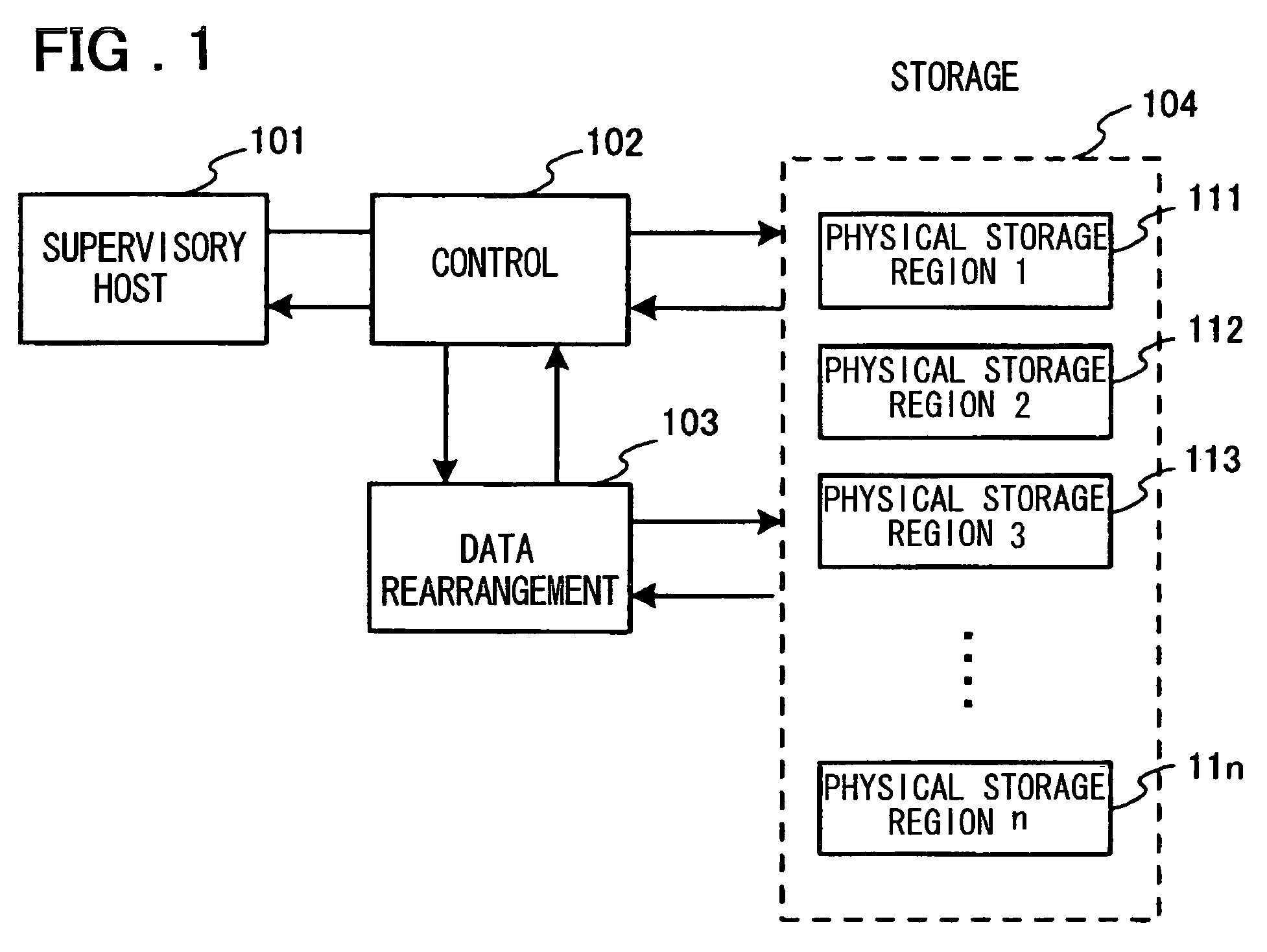
[0045]FIG. 1 is a block diagram of a data storage system showing the present invention.

[0046]The data storage system in this embodiment has storage means (unit) 104 including n physically divided storage regions constituted from a physical storage region 111, a physical storage region 112, and a physical storage region 11n. Each physical storage region is the storage region having a group of functions that simultaneously operate during either or all of operations such as data writing, data reading, and data erasure, and shows a group of areas in which various defects may occur. These defects include a defect at the time of manufacture, a malfunction generated in a specific area such as damage caused by electrical migration or static electricity, a defective control circuit, and a malfunction caused by the influence of stability of a supply voltage.

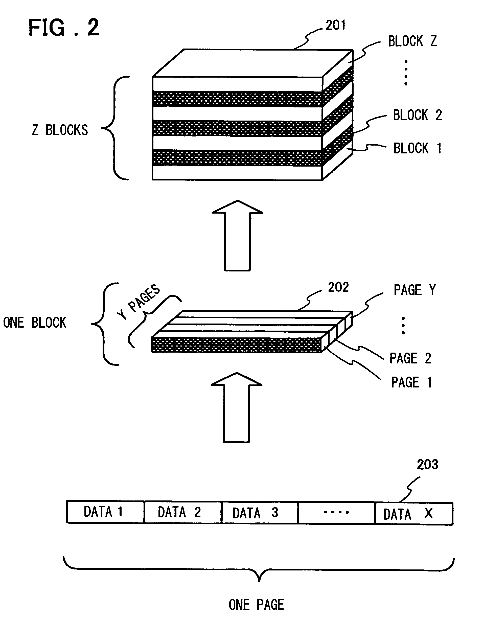
[0047]FIG. 2 shows a configuration of data storage in a flash memory. In the flash memory, a minimum unit of data for data reading such a...

second embodiment

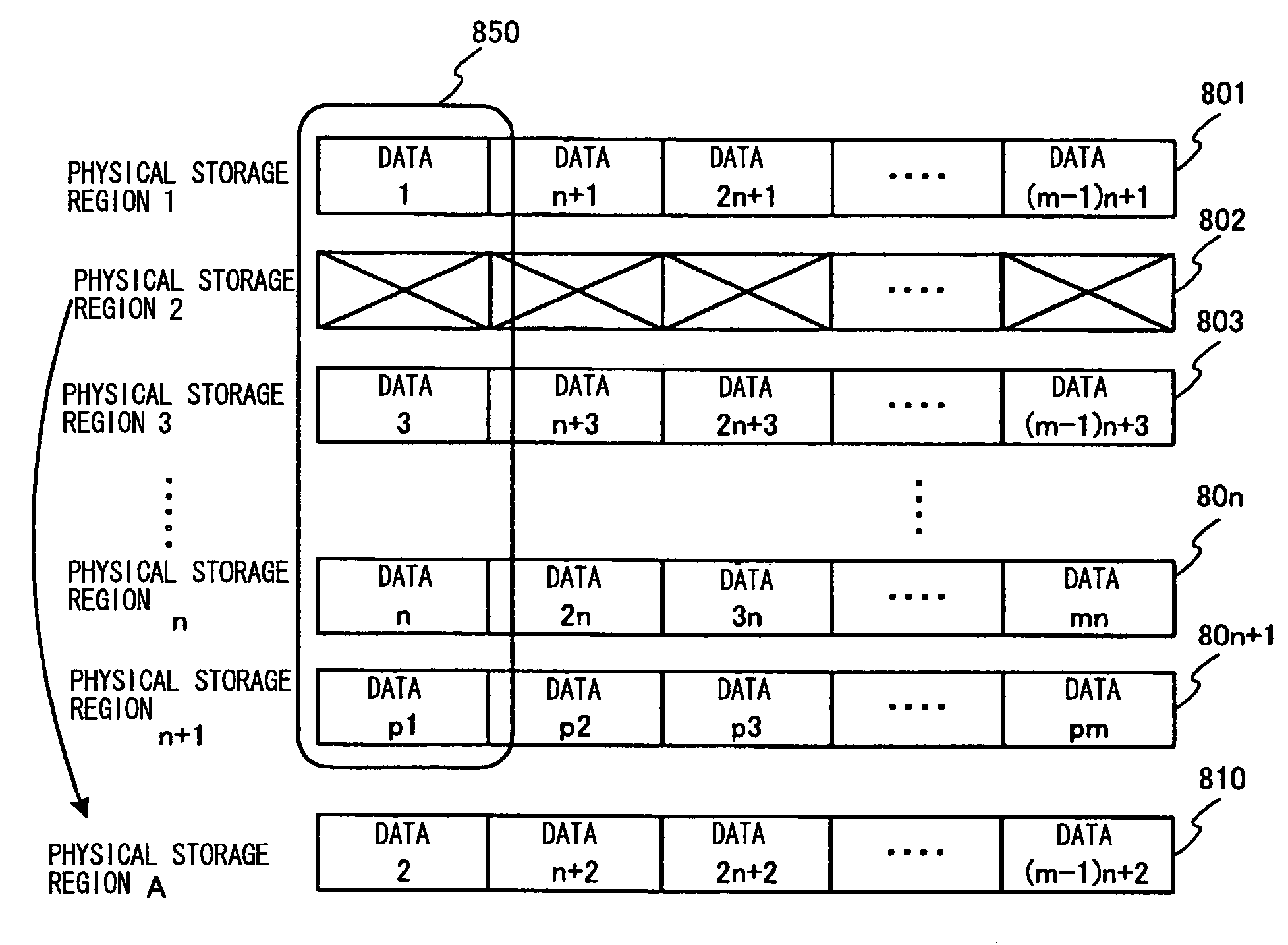
[0068]FIG. 7 is a diagram showing the present invention, and a method of storing data and error correction data in this embodiment. FIG. 8 shows an alternative image of a physical storage region when an error occurs, in this embodiment.

[0069]Generally, in the flash memory or the like, error detection and error correction are performed by adding redundant data such as a parity to each arbitrary data unit for data error correction. Part or all of data to be paired with this error correction data is stored in one physical storage region. Thus, when a data error or the like has occurred due to a defect in the physical storage region, there arises the problem that most of a group of data stored in this physical storage region is lost and execution of the error correction thereby becomes impossible.

[0070]In this embodiment, a sequence of data is split across and spread over a plurality of physical storage regions for storage without being stored in the unit of one physical storage region,...


PUM


Abstract

Reliability of stored data in a semiconductor storage device such as a flash memory is enhanced. There are provided (n+1) physical storage regions each having m data storage areas and for which data writing, data reading, data erasure, and the like are collectively performed. A sequence of data input from a supervisory host as write data are rearranged, and that sequence of data is split across the n physical storage regions, for storage. Error correction data for the sequence of data 1 to data n split across the respective physical storage regions is stored in another (n+1)th physical storage region as data p1. Error correction data p2 for data (n+1) to data 2n, and error correction data pm for data ((m−1)n+1) to data mn are stored in the same manner. When abnormality is present in part or all of the data stored in a second physical storage region, for example, the data in the second physical storage region restored by error correction is stored in an alternative physical storage region, and the data in the second physical storage region are all erased.

Description

FIELD OF THE INVENTION[0001]The present invention relates to a method of data writing to and data reading from a storage device. More specifically, the invention relates to the method of data writing to and data reading from a semiconductor memory device such as a flash memory.BACKGROUND OF THE INVENTION[0002]The storage capacity of a data storage device typified by a semiconductor memory in an information device such as a computer, a PDA (Personal Data Assistance, Personal Digital Assistants: Personal Portable Type Information Communication Device), a household game device, a digital camera, or a cellular phone, or a PHS (Personal Hand-phone System) keeps on increasing year by year. The flash memory in particular, which is a ROM (Read Only Memory) that can perform electrical erasure of and electrical writing to storage, is a nonvolatile memory from which the storage does not vanish even if external power is not supplied thereto, and is used a lot in various fields.[0003]The flash m...

Claims


Application Information

Patent Timeline
Patent Type & Authority Patents(United States)
IPC IPC(8): G06F11/00G06F11/10G06F12/16
CPCG06F11/108
Inventor TACHIKAWA, TAKASHI
Owner LENOVO INNOVATIONS LTD HONG KONG
Why Eureka
Try Eureka