Flexible printed circuit board for electronic equipment

a printed circuit board and electronic equipment technology, applied in printed circuit details, printed circuits, electrical equipment, etc., can solve the problems of increasing manufacturing costs of shield tape or shield foam, and achieve the effects of preventing circuit damage, reducing product failure rate, and improving assembly process

Inactive Publication Date: 2008-11-04
SAMSUNG ELECTRONICS CO LTD
View PDF17 Cites 6 Cited by
  • Summary
  • Abstract
  • Description
  • Claims
  • Application Information

AI Technical Summary

Benefits of technology

[0022]Therefore, an object of the present invention is to provide a flexible printed circuit board (FPCB) for electronic equipment, in which a second plating interface 70, instead of a first plating interface inside a compression part of the FPCB, is folded by a force generated when a connector of the FPCB is engaged, thereby preventing circuit damage, improving an assembly process, and reducing a product failure rate.
[0023]Another object of the present invention is to provide a flexible printed circuit board (FPCB) for electronic equipment, in which a folding part is folded by a force generated when a connector of the FPCB is engaged, thereby reducing product manufacturing cost through no need for a separate damage prevention member in the FPCB.

Problems solved by technology

At this time, the first plating interface may be damaged when being folded, causing degradation in a process of assembling the FPCB.
However, the additional process of adhering the shield tape or shield foam increases time, and the additional use of the shield tape or shield foam increases manufacturing cost.
As a result, repetitive sliding causes intensive rotation or folding and thus cracks at the compression part 60 of the circuit connector 41 and the first plating interface form.

Method used


Image

  • Flexible printed circuit board for electronic equipment
  • Flexible printed circuit board for electronic equipment
  • Flexible printed circuit board for electronic equipment

Examples


Embodiment Construction

[0036]Exemplary embodiments of the present invention will now be described in detail with reference to the accompanying drawings.

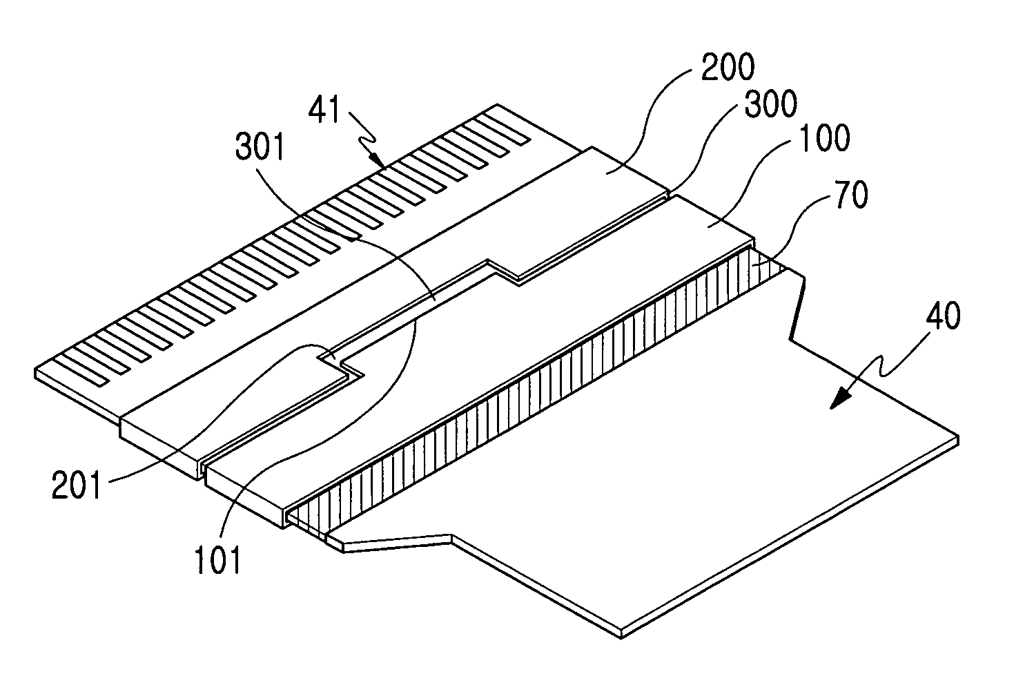
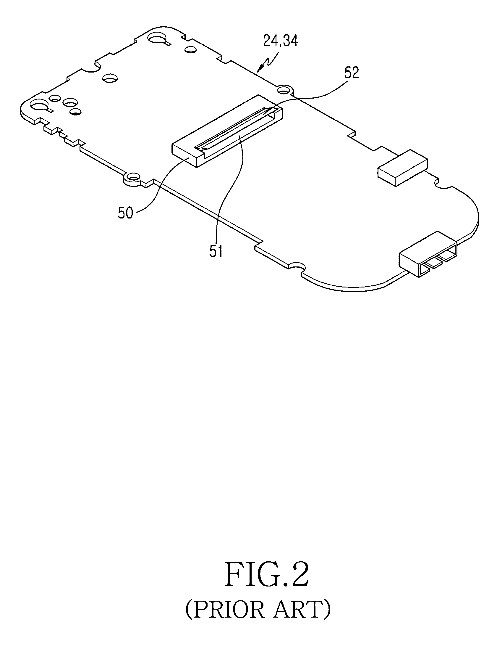
[0037]As illustrated in FIG. 6, a circuit board connector 50 is included in a printed circuit board (PCB) 24 and a liquid crystal display (LCD) PCB 34 of electronic equipment 10, and a flexible printed circuit board (FPCB) 40 comprising a circuit connector 41 connected to the circuit board connector 50 is provided.

[0038]The FPCB 40 comprises a first compression part 100 and a second compression part 200 whose surfaces are processed electrolytic copper. The first compression part 100 and the second compression part 200 are adhered to the FPCB 40 by an adhesive (not shown). A plating interface 70 (hereafter, referring to a second plating interface) is provided adjacent to the first compression part 100.

[0039]As illustrated in FIG. 6, a folding part 300 is provided at a plating interface (hereafter, a first plating interface) between the first compression par...


PUM


Abstract

Provided is a flexible printed circuit board (FPCB) including a circuit connector connected to a circuit board connector of a printed circuit board (PCB) for electronic equipment. A first compression part and a second compression part are included in the circuit connector, and a folding part is provided at a first plating interface between the first compression part and the second compression part such that a second plating interface, instead of a first plating interface of the first compression part and the second compression part, is folded by a force generated when the circuit connector is connected to the circuit board connector.

Description

PRIORITY[0001]This application claims the benefit under 35 U.S.C. § 119(a) of a Korean Patent Application entitled “Flexible Printed Circuit Board for Electronic Equipment” filed in the Korean Intellectual Property Office on Jun. 7, 2005 and assigned Serial No. 2005-48281, the entire contents of which are hereby incorporated by reference.BACKGROUND OF THE INVENTION[0002]1. Field of the Invention[0003]The present invention generally relates to a flexible printed circuit board for electronic equipment. In particular, the present invention relates to a flexible printed circuit board for electronic equipment, in which a folding part is folded by a force generated when a connector included in the flexible printed circuit board is engaged.[0004]2. Description of the Related Art[0005]In general, the term “portable communication apparatus” means an electronic apparatus which a user can carry with him / her to perform wireless communication with another party. As examples of the portable commu...

Claims


Application Information

Patent Timeline
Patent Type & Authority Patents(United States)
IPC IPC(8): H05K1/00
CPCH05K1/028H05K3/244H05K3/281H05K1/02
Inventor KIM, SANG-BO
Owner SAMSUNG ELECTRONICS CO LTD
Why Eureka
Try Eureka