Eureka AIR delivers breakthrough ideas for toughest innovation challenges, trusted by R&D personnel around the world.

Adhesive film for semiconductor, metal sheet with such adhesive film, wiring substrate with adhesive film, semiconductor device, and method for manufacturing semiconductor device

a technology for adhesive films and semiconductors, applied in semiconductor devices, semiconductor/solid-state device details, thin material processing, etc., can solve the problems of fine wiring not being formed and still high, and achieve the effect of sufficient adhesive strength and easy peeling

Active Publication Date: 2008-11-11
RESONAC CORPORATION
View PDF11 Cites 7 Cited by
  • Summary
  • Abstract
  • Description
  • Claims
  • Application Information

AI Technical Summary

Benefits of technology

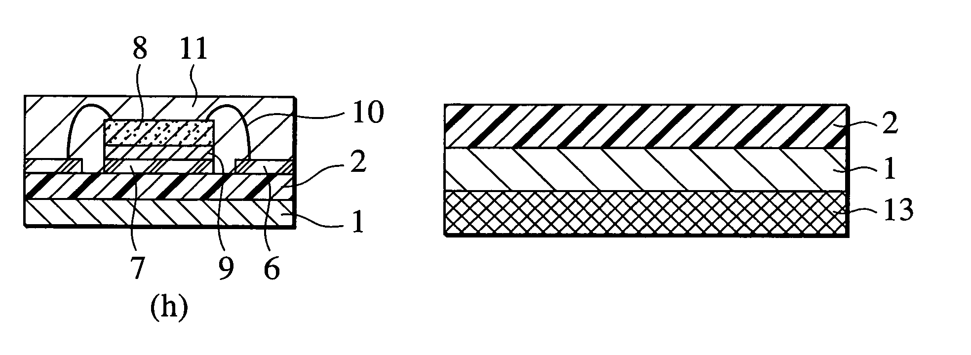
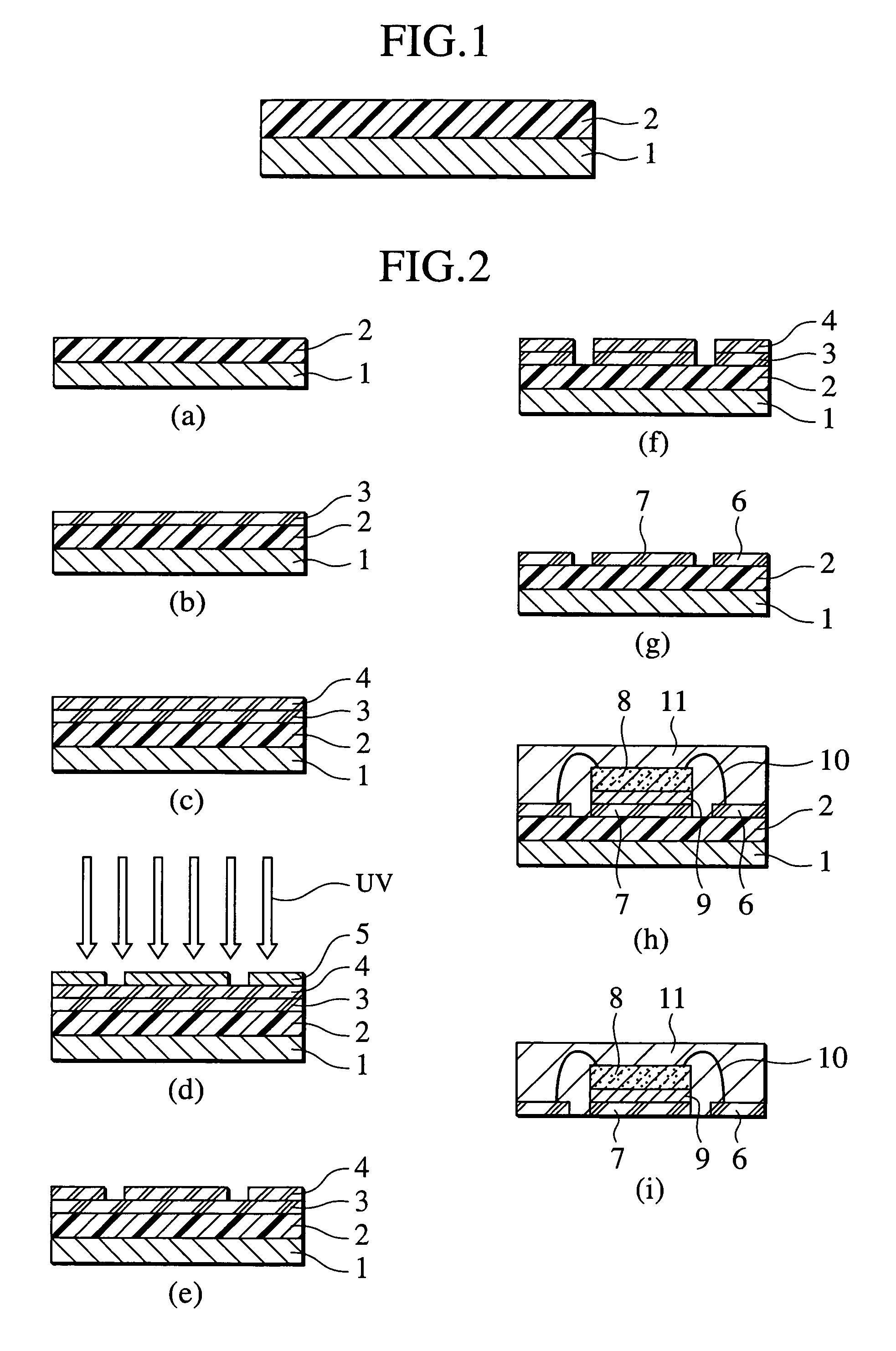
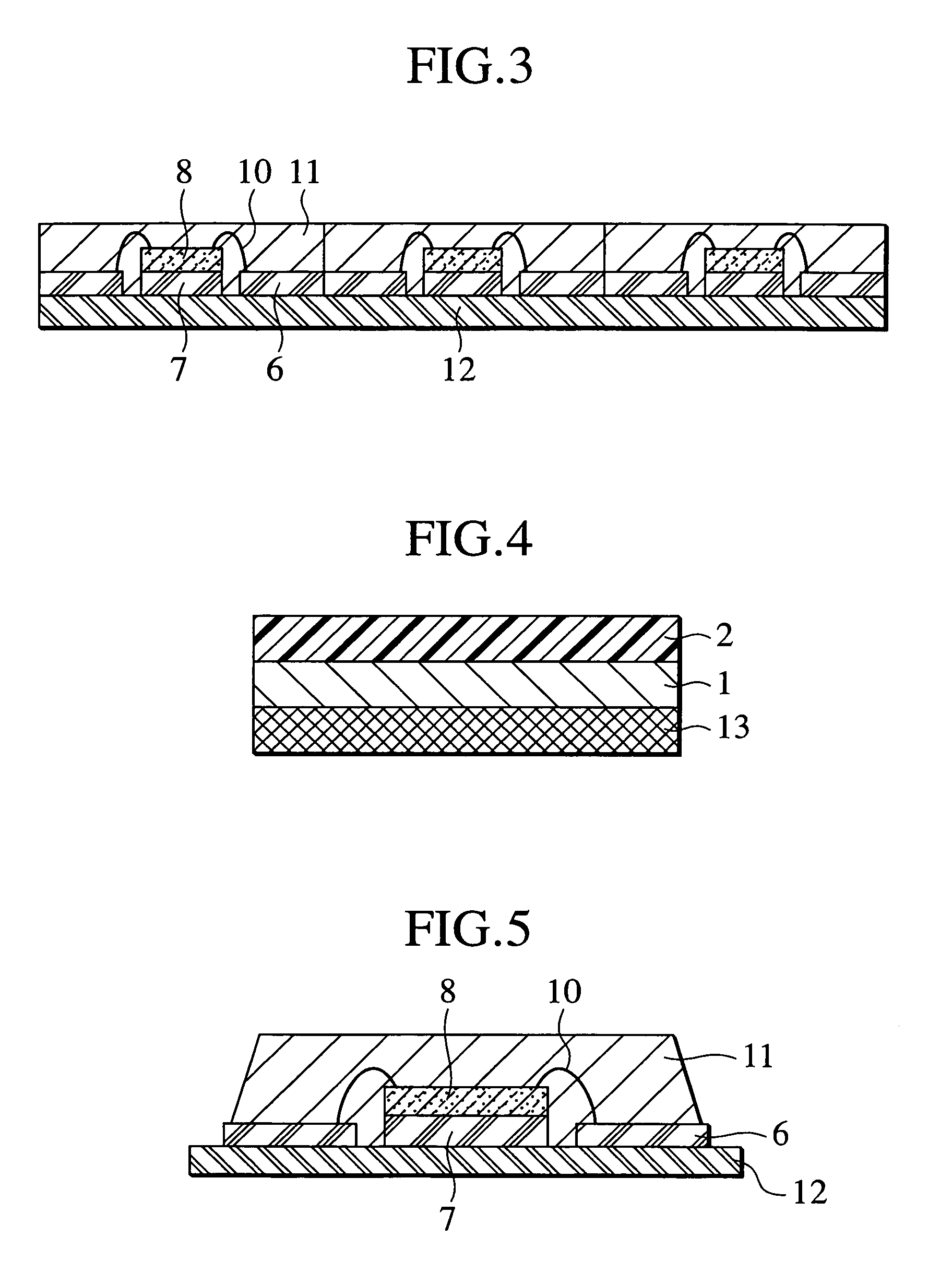
[0004]It is an object of the present invention to provide an adhesive film for semiconductor use that has sufficient adhesive strength to a metal sheet, can be easily peeled off after molding with a resin, and possesses various properties required for semiconductor applications, and to provide a metal sheet laminated with the adhesive film, a wiring circuit laminated with the adhesive film, and a semiconductor device using the adhesive film.
[0005]It is also an object of the present invention to provide a method for producing a semiconductor device, the method enabling a high density and small area and thickness semiconductor device to be produced with excellent productivity.

Problems solved by technology

However, when a lead frame is used, there are restrictions on the thickness and the material of the lead frame, and there are the problems that the semiconductor package is still high, fine wiring cannot be formed, etc.

Method used


Image

  • Adhesive film for semiconductor, metal sheet with such adhesive film, wiring substrate with adhesive film, semiconductor device, and method for manufacturing semiconductor device
  • Adhesive film for semiconductor, metal sheet with such adhesive film, wiring substrate with adhesive film, semiconductor device, and method for manufacturing semiconductor device
  • Adhesive film for semiconductor, metal sheet with such adhesive film, wiring substrate with adhesive film, semiconductor device, and method for manufacturing semiconductor device

Examples


production example 1

Production of Aromatic Polyetheramideimide Adhesive Varnish for Use in Examples 1 to 4, 7, and 8

[0102]A 5 L four-necked flask equipped with a thermometer, a stirrer, a nitrogen inlet, and a fractionating column was charged under an atmosphere of nitrogen with 258.3 g (0.63 mol) of 2,2-bis[4-(4-aminophenoxy)phenyl]propane and 10.4 g (0.042 mol) of 1,3-bis(3-aminopropyl)tetramethyldisiloxane, which were then dissolved in 1450 g of N-methyl-2-pyrrolidone. This solution was heated to 70° C., and 33.6 g (0.168 mol) of 1,12-diaminododecane was dissolved therein. This solution was then cooled to 0° C., and 180.4 g (0.857 mol) of trimellitic anhydride chloride was added thereto. When the trimellitic anhydride chloride dissolved, 130 g of triethylamine was added. Stirring was continued at room temperature for 2 hours, the mixture was then heated to 180° C., and a reaction was carried out for 5 hours so as to complete imidization. The reaction mixture thus obtained was poured into methanol so...

production example 2

Production of Aromatic Polyetheramideimide Adhesive Varnish for Use in Examples 5 and 6

[0103]A 5 L four-necked flask equipped with a thermometer, a stirrer, a nitrogen inlet, and a fractionating column was charged under an atmosphere of nitrogen with 258.6 g (0.63 mol) of 2,2-bis[4-(4-aminophenoxy)phenyl]propane and 67.0 g (0.27 mol) of 1,3-bis(3-aminopropyl)tetramethyldisiloxane, which were then dissolved in 1550 g of N-methyl-2-pyrrolidone. This solution was then cooled to 0° C., and 187.3 g (0.89 mol) of trimellitic anhydride chloride was added thereto at this temperature. When the trimellitic anhydride chloride dissolved, 100 g of triethylamine was added. Stirring was continued at room temperature for 2 hours, the mixture was then heated to 180° C., and a reaction was carried out for 5 hours so as to complete imidization. The reaction mixture thus obtained was poured into methanol so as to isolate a polymer. This polymer was dried and then dissolved in N-methyl-2-pyrrolidone, an...

production example 3

Production of Aromatic Polyetheramideimide Varnish for Use in Resin Layer B in Example 5

[0104]A 5 L four-necked flask equipped with a thermometer, a stirrer, a nitrogen inlet, and a fractionating column was charged under an atmosphere of nitrogen with 172.4 g (0.42 mol) of 2,2-bis[4-(4-aminophenoxy)phenyl]propane and 153.7 g (0.42 mol) of 4,4′-methylenebis(2,6-diisopropylaniline), which were then dissolved in 1550 g of N-methyl-2-pyrrolidone. This solution was then cooled to 0° C., and 174.7 g (0.83 mol) of trimellitic anhydride chloride was added thereto at this temperature. When the trimellitic anhydride chloride dissolved, 130 g of triethylamine was added. Stirring was continued at room temperature for 2 hours, the mixture was then heated to 180° C., and a reaction was carried out for 5 hours so as to complete imidization. The reaction mixture thus obtained was poured into methanol so as to isolate a polymer. This polymer was dried and then dissolved in N-methyl-2-pyrrolidone, an...


PUM


Abstract

An adhesive film for semiconductor use of the present invention is used in a method in which, after the adhesive film for semiconductor use is laminated to one side of a metal sheet, the metal sheet is processed to give a wiring circuit, a semiconductor die is mounted and molded, and the adhesive film is then peeled off. The adhesive film includes a resin layer A formed on one side or both sides of a support film, the 90 degree peel strength between the resin layer A and the metal sheet prior to the processing of the metal sheet laminated with the adhesive film for semiconductor use to give the wiring circuit is 20 N / m or greater at 25° C., and the 90 degree peel strengths, after molding with a molding compound the wiring circuit laminated with the adhesive film for semiconductor use, between the resin layer A and the wiring circuit and between the resin layer A and the molding compound are both 1000 N / m or less at at least one point in the temperature range of 0° C. to 250° C.

Description

TECHNICAL FIELD[0001]The present invention relates to an adhesive film for semiconductor use that enables a semiconductor package to be produced with high workability since the adhesive film can be peeled off easily from a wiring circuit and a molding resin; a metal sheet laminated with the adhesive film, a wiring circuit laminated with the adhesive film, and a semiconductor device that employ the adhesive film for semiconductor use; and a method for producing a semiconductor device.BACKGROUND ART[0002]In order to achieve a smaller, thinner semiconductor package, a package having a structure in which only one side (semiconductor die side) of a lead frame is molded and exposed leads on the reverse side are used for external connection has been developed in recent years. A package with this structure has the advantages of achieving a smaller, thinner semiconductor package since the leads do not project from a molding resin. For example, a method in which, after an adhesive tape is lam...

Claims


Application Information

Patent Timeline
Patent Type & Authority Patents(United States)
IPC IPC(8): H01L21/00H01L21/56H01L21/68H01L23/31
CPCH01L21/561H01L24/97H01L21/568Y10T428/2839H01L23/3107H01L2221/68309H01L2221/68345H01L2221/68359H01L2224/32245H01L2224/48091H01L2224/48247H01L2224/73265H01L2224/97H01L2924/01004H01L2924/01013H01L2924/01015H01L2924/01016H01L2924/01027H01L2924/01029H01L2924/01033H01L2924/0104H01L2924/01046H01L2924/01047H01L2924/01058H01L2924/01078H01L2924/01079H01L2924/01082H01L2924/09701H01L2224/45144H01L2924/01006H01L2924/01005H01L2224/85H01L2924/00014H01L2224/83H01L2924/00H01L2924/181Y10T428/31678H01L2924/00012
Inventor MATSUURA, HIDEKAZUKAWAI, TOSHIYASU
Owner RESONAC CORPORATION
Why Eureka
Eureka Blog
Learn More