Bond quality indication by bump structure on substrate

a bump structure and substrate technology, applied in semiconductor/solid-state device testing/measurement, semiconductor device details, semiconductor devices, etc., can solve the problems of conductive particles that are mostly unbroken and electrically non-conductive, conductive particles may be over-compressed, and the analysis method wastes a lot of time, so as to determine the gap instantaneously

Inactive Publication Date: 2008-11-11
TAIWAN TFT LCD ASSOC +6
View PDF5 Cites 11 Cited by
  • Summary
  • Abstract
  • Description
  • Claims
  • Application Information

AI Technical Summary

Benefits of technology

[0010]The present invention is directed to a bump structure on a substrate. The bump structure can be utilized to instantly determine size of the gap between a glass substrate and a chip and bonding process quality.

Problems solved by technology

However, this method of analysis wastes a lot of time.
When the bonding is inadequate, the conductive particles are mostly unbroken and electrically non-conductive.
On the contrary, if the bonding force is too large, the conductive particles may be over-compressed.
The over-compression may lead to a non-conductive condition.
However, this method cannot measure the size of the gap between the chip and the glass substrate effectively and instantaneously.
However, this method cannot measure the size of the gap between the glass substrate and the chip.

Method used


Image

  • Bond quality indication by bump structure on substrate
  • Bond quality indication by bump structure on substrate
  • Bond quality indication by bump structure on substrate

Examples


first embodiment

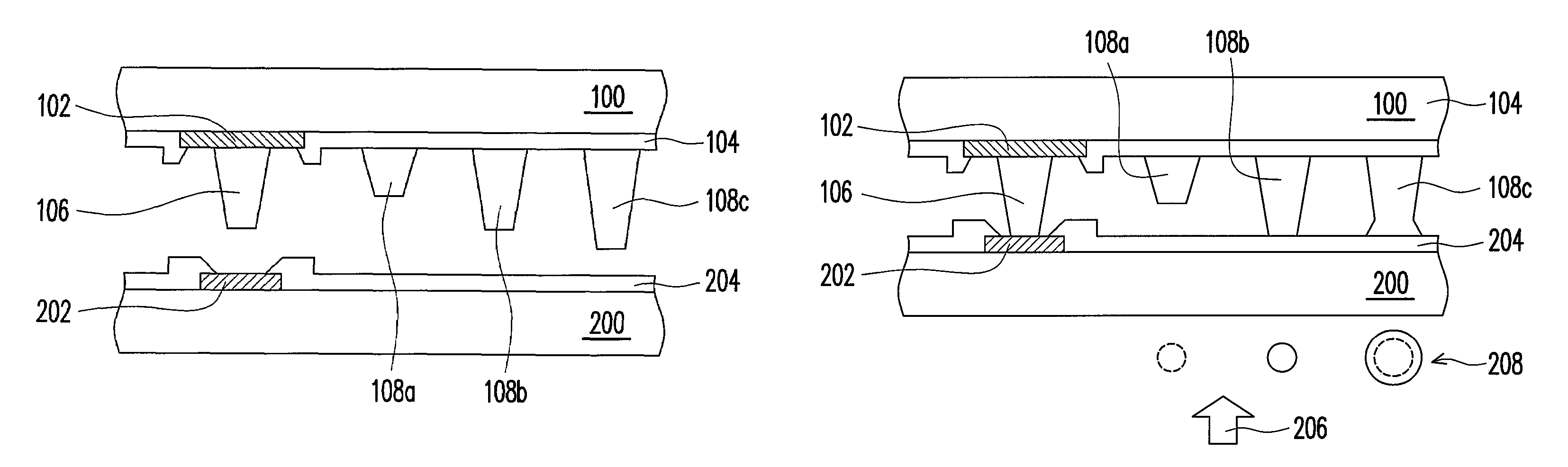
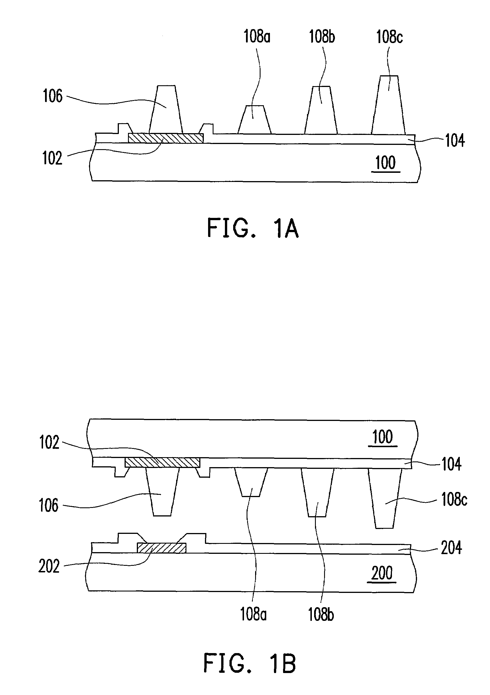
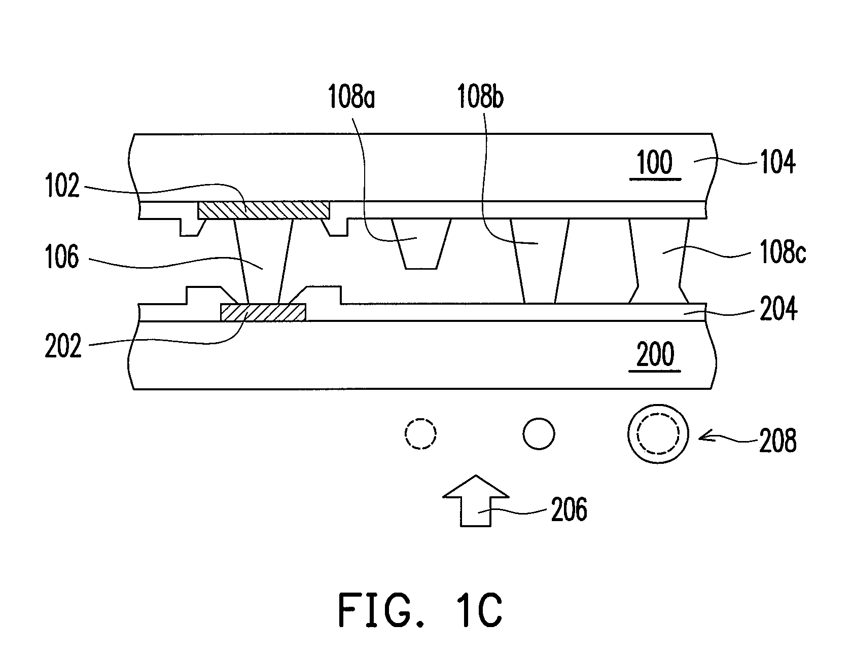
[0029]FIGS. 1A to 1C are schematic cross-sectional views showing a bump structure on a substrate and a corresponding bonding process according to an embodiment of the present invention. As shown in FIG. 1A, the bump structure in the present embodiment is disposed on a substrate 100. The bump structure includes at least one electrode 102, a first bump 106 and a plurality of second bumps 108a, 108b and 108c. In one preferred embodiment, the electrode 102 is formed on the substrate 100. Furthermore, the surface of the substrate 100 further includes a passivation layer 104 that exposes the electrode 102. The substrate 100 is a silicon substrate, a glass substrate, a printed circuit board, a flexible substrate or a ceramic substrate, for example. The material of the electrode 102 is a metal, for example. The first bump 106 is located on the electrode 102. The second bumps 108a, 108b and 108c are located on the substrate 100. In other words, the second bumps 108a, 108b and 108c are locate...

second embodiment

[0041]FIGS. 8A to 8C are schematic cross-sectional views showing a bump structure on a substrate and a corresponding bonding process according to another embodiment of the present invention. As shown in FIG. 8, the bump structure of the present embodiment is disposed on a substrate 100 and includes at least one electrode 102 and at least one staircase-shape bump 306. In a preferred embodiment, the electrode 102 is formed on the substrate 100. Furthermore, a passivation layer 104 is also formed on the surface of the substrate 100. The passivation layer 104 exposes the electrode 102. In the present embodiment, the staircase-shape bump 306 is located on the electrode 102. Similarly, the staircase-shape bump 306 can be a metal bump, a conductive bump or an elastic bump comprising a polymer bump and a conductive layer on the polymer bump. In addition, the horizontal cross-section of the staircase-shape bump 306 is a circle, an ellipse, a rectangle or a polygon. The staircase-shape bump 3...


PUM


Abstract

A bump structure on a substrate including at least one first electrode, at least one first bump, at least one second bump is provided. The first electrode is disposed on the substrate. The first bump is disposed on the first electrode. The second bump is disposed on the substrate. The height of the second bump is greater than that of the first bump. The elastic bump of the present invention can be used for measuring the bonding process quality.

Description

CROSS-REFERENCE TO RELATED APPLICATION[0001]This application claims the priority benefit of Taiwan application serial no. 96106105, filed Feb. 16, 2007. All disclosure of the Taiwan application is incorporated herein by reference.BACKGROUND OF THE INVENTION[0002]1. Field of the Invention[0003]The present invention generally relates to a bump structure on a substrate, in particular, to a bump structure for measuring bonding process quality.[0004]2. Description of Related Art[0005]In general, size of the gap between a glass substrate and a chip in a chip-on-glass (COG) process is determined by several factors including processing pressure, properties of plastic, stress relieve and so on. To determine the foregoing processing parameters, the selection of the gap between the chip and the glass substrate is particularly important. At present, the size of the gap between the glass substrate and the chip can be determined by performing a slice-up analysis using a scanning electron microsco...

Claims


Application Information

Patent Timeline
Patent Type & Authority Patents(United States)
IPC IPC(8): H01L23/58H01L23/544
CPCH01L22/12H01L23/49816H01L24/13H01L24/14H01L24/81H01L2223/54426H01L2224/0401H01L2224/0603H01L2224/06505H01L2224/10135H01L2224/13012H01L2224/13016H01L2224/13099H01L2224/1403H01L2224/14505H01L2224/16H01L2224/81136H01L2224/81139H01L2224/81801H01L2924/01082H01L2924/01033H01L2224/14051H01L2224/81191H01L2224/131H01L2224/1319H01L2924/00014H01L2924/15787H01L2224/13013H01L2224/13014H01L2924/00H01L2924/00012
Inventor CHEN, MING-YAOYANG, SHENG-SHUCHANG, SHYH-MINGTSANG, NGAI
Owner TAIWAN TFT LCD ASSOC
Why Eureka
Try Eureka