Non-volatile memory device and method having bit-state assignments selected to minimize signal coupling

a non-volatile memory and bit-state assignment technology, applied in static storage, digital storage, instruments, etc., can solve the problems of data storage errors, the precision with which circuitry can store analog values on floating gates of flash cells, and the inability to store data in the same way across flash cells across an array and even across a single row

Active Publication Date: 2008-11-25
MICRON TECH INC
View PDF19 Cites 40 Cited by
  • Summary
  • Abstract
  • Description
  • Claims
  • Application Information

AI Technical Summary

Problems solved by technology

There is also a limit to the precision with which circuitry can store an analog value on the floating gate of a flash cell, particularly where multiple levels of charge must be stored.
In particular, because of process variations, the flash cells across an entire array and even across a single row may not all behave identically.
These program disturb effects can increase the charge stored on the floating gates of memory cells in the row that either have been programmed or are being programmed to a lower charge level, thereby resulting in data storage errors.
Similarly, an increase in the voltage of a floating gate caused by programming a selected memory cell can be coupled to the floating gate of an adjacent non-selected memory cell, thereby also inadvertently affecting the charge stored on the floating gate of the non-selected memory cell.
However, these types of floating gate-to-floating gate and program disturb problems or similar problems can also exist when programming single-level flash memory cells and possibly other types of volatile memory devices.
Therefore, higher programming voltages tend to induce a greater degree of floating gate-to-floating gate coupling and program disturb effects.
Unfortunately, the magnitude of a programming voltage that must be applied to the control gate of a flash memory cell is fixed by the characteristics of the memory device, the number of charge levels to which each cell can be programmed in a multi-level memory cell, and the bit set to which the cell is to be programmed.

Method used


Image

  • Non-volatile memory device and method having bit-state assignments selected to minimize signal coupling
  • Non-volatile memory device and method having bit-state assignments selected to minimize signal coupling
  • Non-volatile memory device and method having bit-state assignments selected to minimize signal coupling

Examples


Embodiment Construction

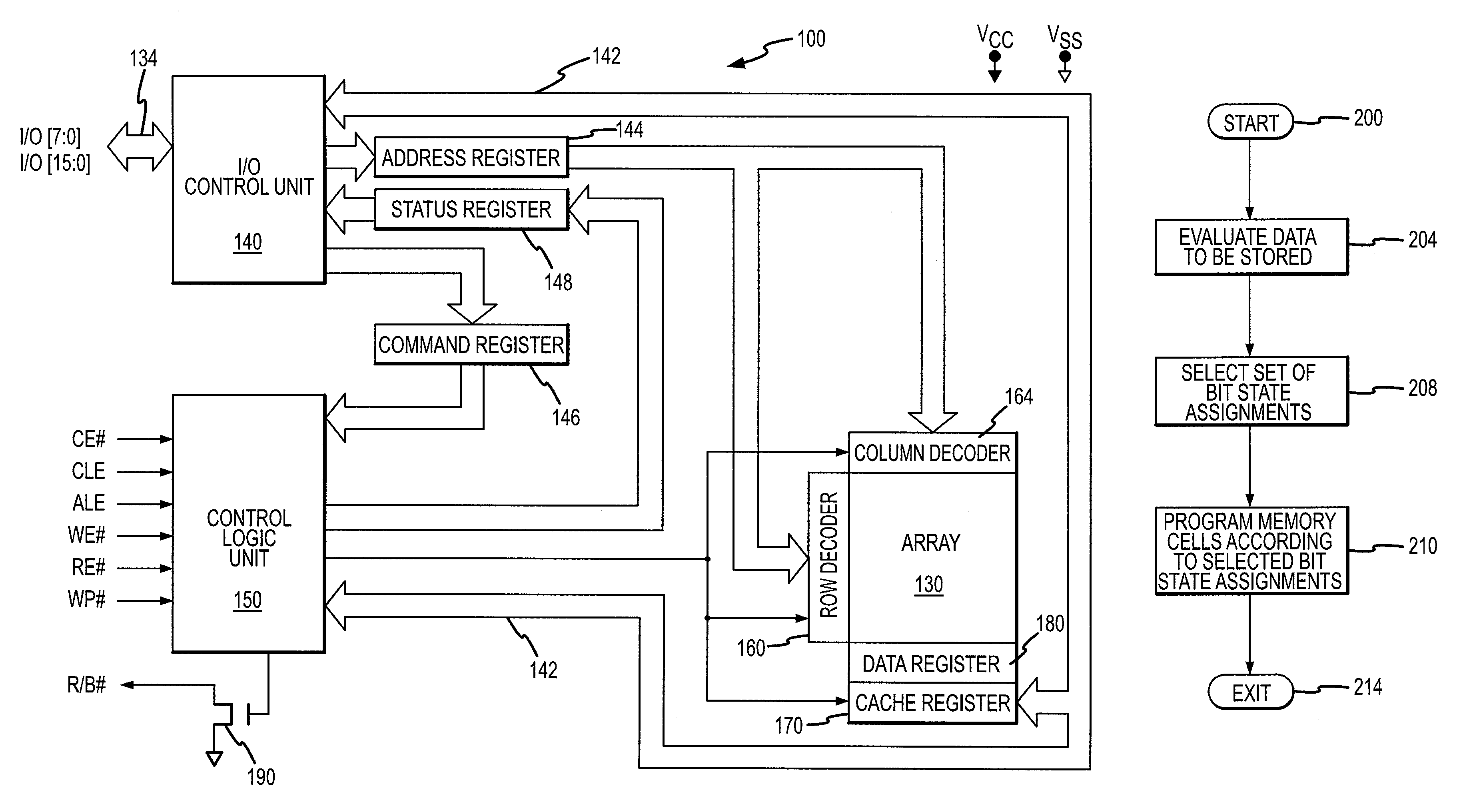
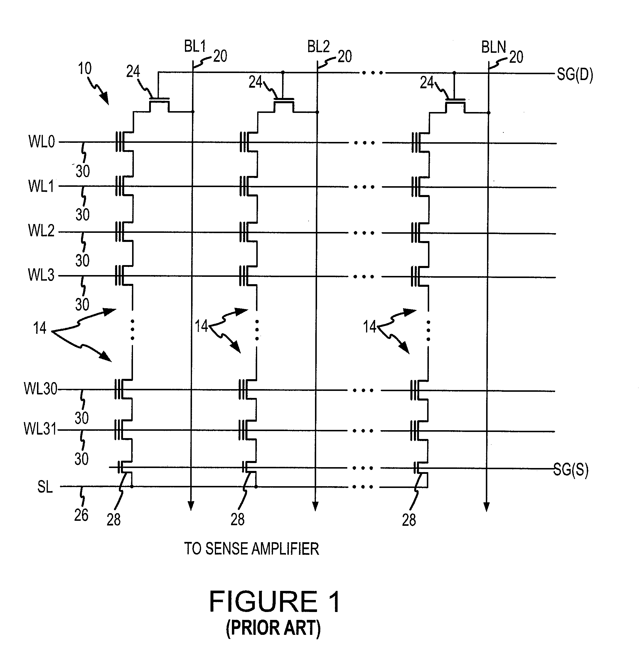
[0026]A flash memory device 100 according to one example of the invention is shown in FIG. 3. The flash memory device 100 includes an array 130 of flash memory cells arranged in banks of rows and columns. The flash memory cells in the array 130 have their control gates coupled to word select lines, drain regions coupled to local bit lines, and source regions selectively coupled to a ground potential as shown in FIG. 1.

[0027]Unlike conventional dynamic random access memory (“DRAM”) devices and static random access memory (“SRAM”) devices, command, address and write data signals are not applied to the flash memory device 100 through respective command, address and data buses. Instead, most command signals, the address signals and the write data signals are applied to the memory device 100 as sets of sequential input / output (“I / O”) signals transmitted through an I / O bus 134. Similarly, read data signals are output from the flash memory device 100 through the I / O bus 134. The I / O bus is...


PUM


Abstract

A non-volatile memory device programs memory cells in each row in a manner that minimizes the coupling of spurious signals. A control logic unit programs the cells in a row using a set of bit state assignments chosen by evaluating data that are to be written to the cells in the row. The control logic unit performs this evaluation by determining the number of cells in the row that will be programmed to each of a plurality of bit states corresponding to the write data. The control logic unit then selects a set of bit state assignments that will cause the programming level assigned to each bit state to be inversely proportional to the number of memory cells in the row that are programmed with the bit state. The selected set of bit states is then used to program the memory cells in the row.

Description

TECHNICAL FIELD[0001]This invention relates to non-volatile memory devices, and, more particularly, to a non-volatile memory device in which the bit states assigned to multiple programming levels stored by memory cells are varied on a row-by-row basis to minimize signal coupling.BACKGROUND OF THE INVENTION[0002]Electrically erasable and programmable non-volatile memory devices having arrays of flash memory cells are found in a wide variety of electrical devices. One very common type of erasable and programmable non-volatile memory device is a flash memory device. A flash memory device uses flash memory cell, also known as a floating gate transistor memory cell, that are similar to a field effect transistor, having a source region and a drain region that is spaced apart from the source region to form an intermediate channel region. A floating gate, typically made of doped polysilicon, is disposed over the channel region and is electrically isolated from the channel region by a layer ...

Claims


Application Information

Patent Timeline
Patent Type & Authority Patents(United States)
IPC IPC(8): G11C16/10
CPCG11C11/5628G11C16/0483G11C16/12G11C16/3427G11C16/04G11C16/3418G11C2211/5641G11C2211/5643G11C2211/5647
Inventor NAZARIAN, HAGOP A.
Owner MICRON TECH INC
Why Eureka
Try Eureka