Photoelectric conversion apparatus and image pickup system using photoelectric conversion apparatus

a conversion apparatus and photoelectric technology, applied in the field of photoelectric conversion apparatus and image pickup system, can solve the problems of reducing the frame rate and increasing the time necessary for reading a signal, and achieve the effect of suppressing the occurrence of shading and improving the frame ra

Active Publication Date: 2008-12-09
CANON KK
View PDF14 Cites 99 Cited by
  • Summary
  • Abstract
  • Description
  • Claims
  • Application Information

AI Technical Summary

Benefits of technology

[0008]The present invention improves the frame rate or suppresses the occurrence of shading.

Problems solved by technology

As a result, a problem may occur in that the time necessary for reading a signal is increased and the frame rate is thus reduced.

Method used


Image

  • Photoelectric conversion apparatus and image pickup system using photoelectric conversion apparatus
  • Photoelectric conversion apparatus and image pickup system using photoelectric conversion apparatus
  • Photoelectric conversion apparatus and image pickup system using photoelectric conversion apparatus

Examples


first embodiment

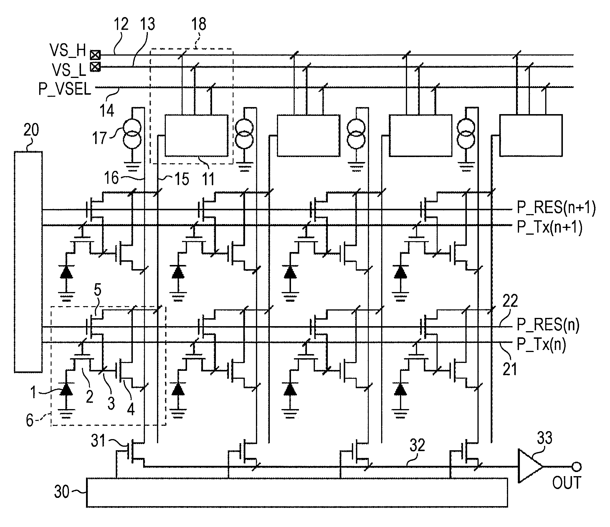
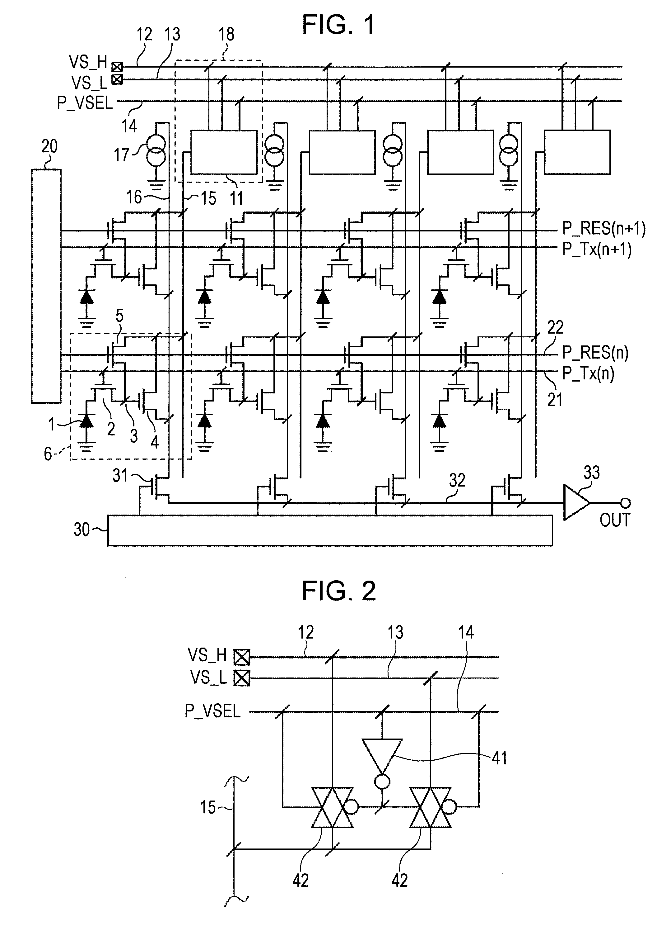
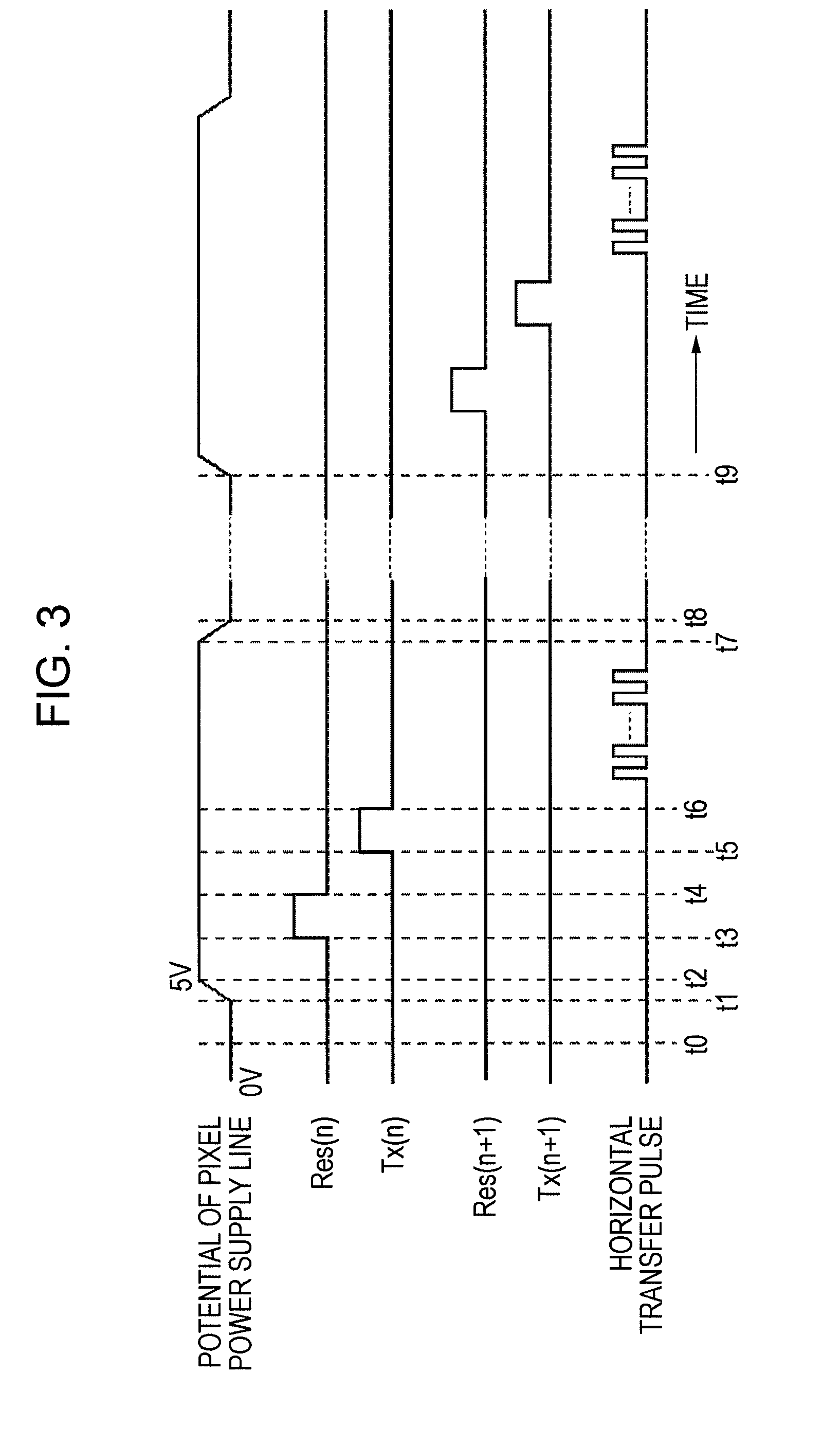
[0031]FIG. 1 is a schematic diagram showing a first embodiment of the present invention. Referring to FIG. 1, eight pixels 6 are arranged two-dimensionally. An area in which the pixels 6 are disposed is referred to as a photoelectric conversion area.

[0032]A photoelectric conversion element 1 converts incident light into an electric charge. A transfer unit 2 transfers the electric charge of the photoelectric conversion element 1 to an input unit 3 for an amplifying unit. The transfer unit 2 may be a MOS transistor. A floating diffusion (FD) region formed on a semiconductor substrate may be used as the input unit 3. A MOS transistor (amplifying MOS transistor) 4 forms the amplifying unit. The gate of the amplifying unit (amplifying MOS transistor) 4 is electrically connected to the input unit (FD region) 3. The amplifying unit (amplifying MOS transistor) 4 is configured as a well-known source follower circuit.

[0033]A voltage supply unit 5 supplies a voltage to the input unit (FD regio...

second embodiment

[0048]FIG. 4 is a schematic diagram showing a second embodiment of the present invention. The second embodiment is different from the first embodiment in the positions of the voltage supply control circuits 11. A feature of the second embodiment is that the voltage supply control circuits 11 are disposed symmetrically to constant-current sources 17, serving as load units connected to the output lines 16, with respect to the photoelectric conversion area. The operation of the photoelectric conversion apparatus according to the second embodiment is similar to that of the first embodiment. Thus, the explanation of the operation of the photoelectric conversion apparatus according to the second embodiment will be omitted.

[0049]With the configuration used in the second embodiment, since the voltage supply control circuits 11 are provided for the individual columns, the frame rate can be improved. In addition, since the influence of power supply deviation caused by coupling of power supply...

third embodiment

[0050]FIG. 5 is a schematic diagram showing a third embodiment of the present invention. The third embodiment is different from the first embodiment in that the voltage supply control circuits 11 are alternately disposed on one side and the other side of the photoelectric conversion area such that a voltage supply control circuit 11 disposed in a column diagonally faces a voltage supply control circuit 11 disposed in an adjacent column across the photoelectric conversion area. Although not illustrated, the voltage supply control circuits 11 may be disposed such that a circuit group including a plurality of voltage supply control circuits 11 diagonally faces an adjacent circuit group including a plurality of voltage supply control circuits 11 across the photoelectric conversion area. The operation of the photoelectric conversion apparatus according to the third embodiment is similar to that of the first embodiment. Thus, the explanation of the operation of the photoelectric conversio...


PUM


Abstract

A photoelectric conversion apparatus includes a photoelectric conversion area in which a plurality of photoelectric conversion elements are arranged to convert incident light into electric charges, a plurality of amplifying units are arranged to read and supply signals based on the electric charges of corresponding photoelectric conversion elements to output lines, a plurality of transfer units are arranged to transfer the electric charges of the corresponding photoelectric conversion elements to input units for corresponding amplifying units, and a plurality of voltage supply units are arranged to supply to corresponding input units voltages for setting the corresponding input units to have first and second potentials are disposed two-dimensionally, and a plurality of voltage supply control units are arranged to supply a voltage to corresponding voltage supply units of the plurality of voltage supply units.

Description

BACKGROUND OF THE INVENTION[0001]1. Field of the Invention[0002]The present invention relates to a photoelectric conversion apparatus and an image pickup system using the photoelectric conversion apparatus.[0003]2. Description of the Related Art[0004]As photoelectric conversion apparatuses used for digital cameras, video cameras, or the like, charge-coupled device (CCD) photoelectric conversion apparatuses or metal-oxide semiconductor (MOS) photoelectric conversion apparatuses have been available. In particular, in recent years, the technological development of complementary metal-oxide semiconductor (CMOS) photoelectric conversion apparatuses has been actively conducted due to advantages of a reduced power consumption and an excellent compatibility with semiconductor processes. Furthermore, in order to satisfy a requirement for increasing the number of pixels and to improve the sensitivity per unit pixel, various configurations in which the number of MOS transistors per unit pixel ...

Claims


Application Information

Patent Timeline
Patent Type & Authority Patents(United States)
IPC IPC(8): H01L27/00H01L27/146H01L31/10H04N5/335H04N5/341H04N5/369H04N5/374
CPCH04N5/3658H04N5/3698H04N5/3741H04N25/677H04N25/709H04N25/766
Inventor KOBAYASHI, MASAHIROITANO, TETSUYA
Owner CANON KK
Why Eureka
Try Eureka