System and method for providing automated sample preparation for plan view transmission electron microscopy

a transmission electron microscopy and automatic technology, applied in the direction of semiconductor devices, semiconductor/solid-state device details, electric discharge tubes, etc., can solve the problems of increasing the time spent on the fib preparation of samples, high cost and common use, and achieve the effect of facilitating the plan view tem imaging of sample wafers

Active Publication Date: 2009-01-20
NAT SEMICON CORP
View PDF0 Cites 2 Cited by
  • Summary
  • Abstract
  • Description
  • Claims
  • Application Information

AI Technical Summary

Benefits of technology

[0024]It is still another object of the present invention to provide a system and method for the automated preparation of sample wafers for plan view TEM imaging to allow laboratory personnel to be free to work on other tasks while the sample wafers of the present invention are automatically being prepared.
[0025]It is another object of the present invention to provide sample wafers that are rotated and remounted on a copper support stub in an orientation that facilitates plan view TEM imaging of the sample wafers.

Problems solved by technology

The chief difficulty associated with TEM has traditionally been the preparation of samples.
The “μ-sampling” technique avoids many of the “pre-preparation” steps such as wafer cleaving, sawing, and tripod polishing, but it does so at the expense of increased time spent on the FIB preparation of the sample.
The high cost and heavy usage commonly associated with FIB instruments make any increase in instrument time for sample preparation a potential factor in bottlenecking laboratory output.
However, there is no similar method for preparing samples for plan view transmission electron microscopy.

Method used


Image

  • System and method for providing automated sample preparation for plan view transmission electron microscopy
  • System and method for providing automated sample preparation for plan view transmission electron microscopy
  • System and method for providing automated sample preparation for plan view transmission electron microscopy

Examples


Embodiment Construction

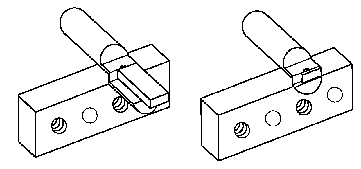
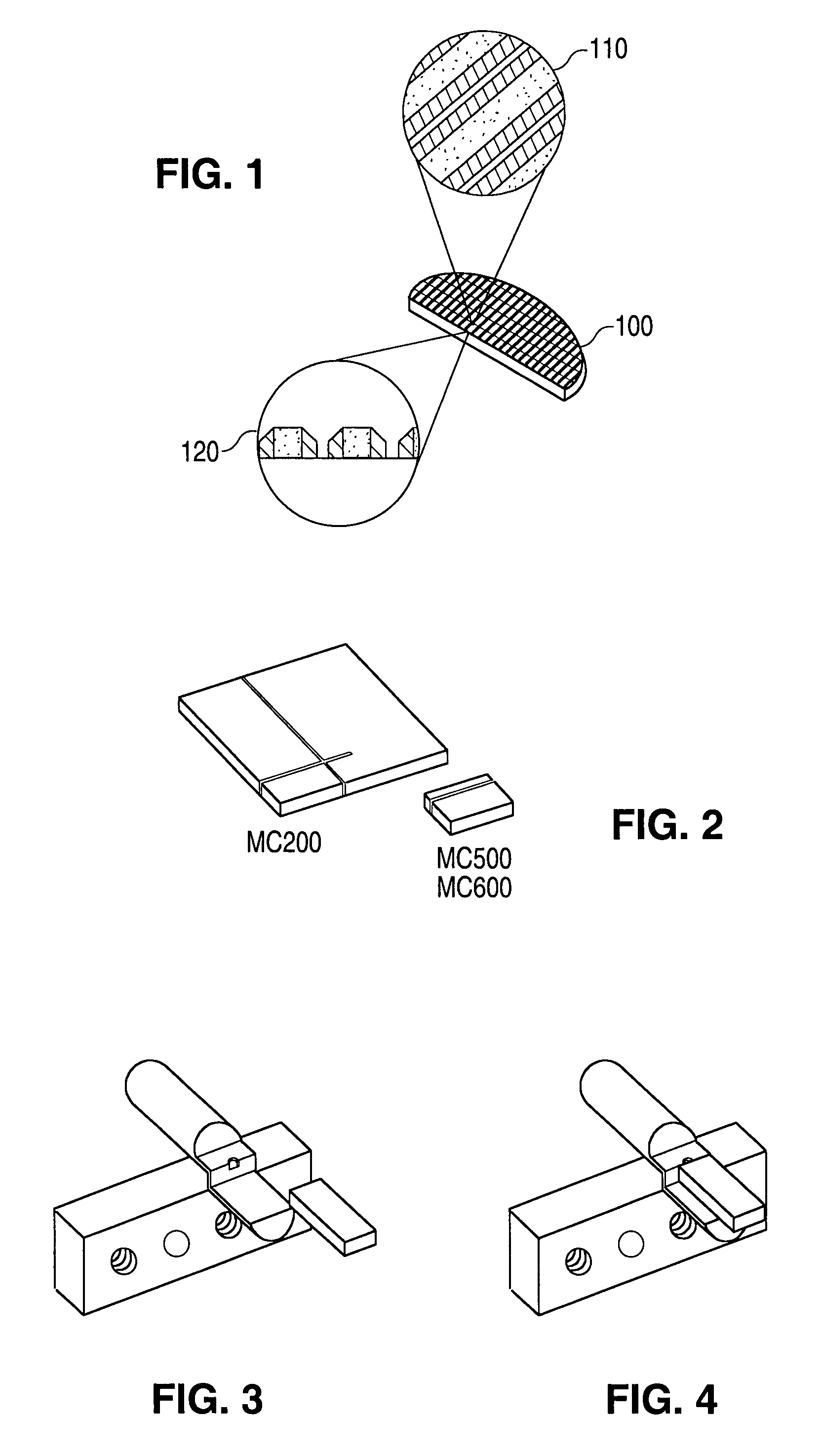
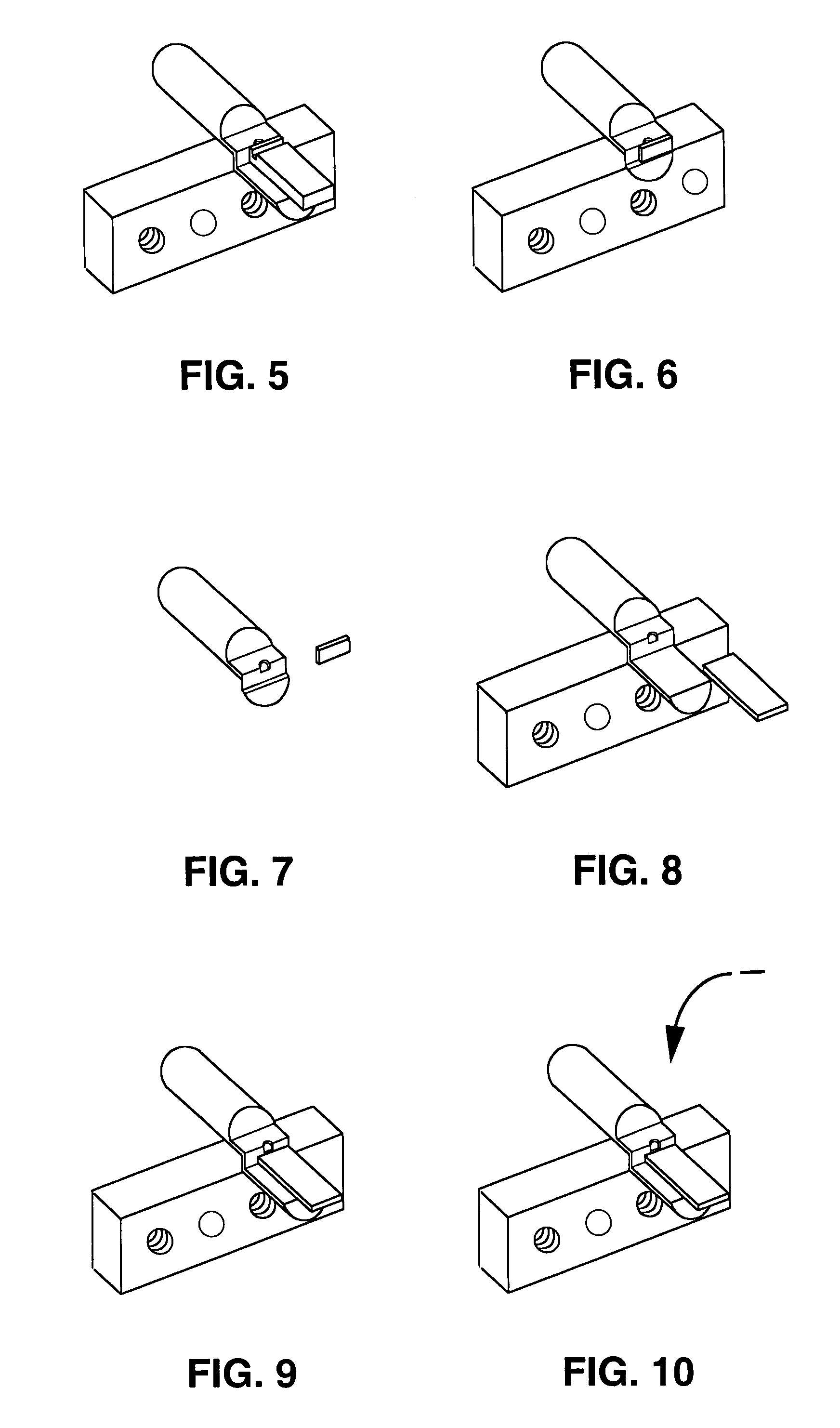
[0053]FIGS. 2 through 24, discussed below, and the various embodiments used to describe the principles of the present invention in this patent document are by way of illustration only and should not be construed in any way to limit the scope of the invention. Those skilled in the art will understand that the principles of the present invention may be implemented in any type of suitably arranged device for preparing plan-view TEM samples.

[0054]To simplify the drawings the reference numerals from previous drawings may sometimes not be repeated for structures that have already been identified.

[0055]The automated plan-view TEM sample preparation method of the present invention comprises a four stage process. The four stages are: (1) microcleaving process, (2) initial sawing process, (3) remounting process, and (4) final sawing process. The resulting TEM sample comprises a thirty micron (30 μm) thick section of silicon wafer glued onto a TEM-compatible support grid, with circuitry contai...


PUM


Abstract

A system and method is described for providing automated sample preparation for plan view transmission electron microscopy. A sample wafer is microcleaved from a semiconductor wafer and mounted on a first support stub. Then the sample wafer is cut with an automated diamond sawing tool to expose a cross sectional view of the sample wafer. The sample wafer is removed from the first support stub and rotated to orient the sample wafer for plan view imaging. The rotated sample wafer is then remounted on a second support stub and cut with the automated diamond sawing tool to expose a plan view surface of the rotated sample wafer. The remounted sample wafer is subsequently prepared for focused ion beam (FIB) milling and plan view transmission electron microscopy imaging.

Description

[0001]This application is a continuation of prior U.S. patent application Ser. No. 10 / 903,367 filed on Jul. 30, 2004, now U.S. Pat. No. 7,250,318.TECHNICAL FIELD OF THE INVENTION[0002]The present invention is generally directed to manufacturing technology for semiconductor circuits and, in particular, to a system and method for providing automated sample preparation for plan view transmission electron microscopy.BACKGROUND OF THE INVENTION[0003]Increasingly smaller geometries and feature sizes of semiconductor devices have made transmission electron microscopy (TEM) an increasing important characterization technique for semiconductor product development and failure analysis. Resolution of less than fifteen hundredths of a nanometer (0.15 nm) allows TEM to provide structural information down to the atomic level. TEM can also be used in conjunction with X-ray or electron energy loss spectrometers to provide information on chemical composition at sub-nanometer length scales. See, for e...

Claims


Application Information

Patent Timeline
Patent Type & Authority Patents(United States)
IPC IPC(8): H01L21/00
CPCG01N23/04H01J2237/2817
Inventor JOHNSON, MARK ALANMAYES, LARRY W.
Owner NAT SEMICON CORP
Why Eureka
Try Eureka