Method of manufacturing GaN crystal substrate

a technology of monocrystalline substrates and monocrystalline crystals, which is applied in the direction of crystal growth process, polycrystalline material growth, chemically reactive gases, etc., can solve the problem of lessening the effective gan crystal portion that can be obtained, and achieves high substrate acquisition rate, increase the effective gan crystal portion, and inhibit the enlargement of the pit size

Inactive Publication Date: 2009-01-27
SUMITOMO ELECTRIC IND LTD
View PDF9 Cites 7 Cited by
  • Summary
  • Abstract
  • Description
  • Claims
  • Application Information

AI Technical Summary

Benefits of technology

[0006]In view of the foregoing circumstances, an object of the present invention is to make available a method of manufacturing GaN crystal substrate that efficiently yields a great amount GaN crystal substrate (that is, in which the substrate-acquisition rate is high) by, in the growing of GaN crystal, inhibiting enlargement of pit size to increase the effective GaN crystal portion in which the grown GaN crystal, separated off in thin, platelike form, is usable as a GaN crystal substrate.

Problems solved by technology

A problem with this pit-employing method of manufacturing GaN crystal substrates, however, has been that along with the GaN crystal growth the pits grow too, enlarging diametrically, which lessens the effective GaN crystal portion that can be obtained by separating off the grown GaN crystal in thin, platelike form.

Method used


Image

  • Method of manufacturing GaN crystal substrate
  • Method of manufacturing GaN crystal substrate
  • Method of manufacturing GaN crystal substrate

Examples


embodiment examples

Examples 1 through 4, Comparative Example 1

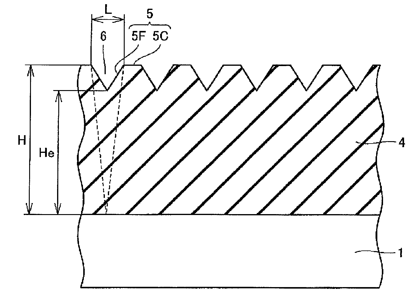
[0039]With reference to FIG. 1, the growing of a GaN crystal 4 was carried out by an HVPE technique using a GaN substrate, which is a native substrate, as a growth substrate 1. The HVPE equipment utilized in the present examples was provided with a boat, disposed inside a reactor, in which Ga metal is accommodated, and was configured to enable introducing HCl gas and a carrier gas directed toward the boat, and, with the growth substrate placed below the boat, to enable introducing NH3 gas and a carrier gas in the vicinity of the growth substrate. A heater was provided on the periphery of the reactor so that the boat and the growth substrate could be heated. An exhaust port is provided below the reactor, and the pressure is reduced by a vacuum pump. A Ga melt in the boat that is heated at 850° C. or higher reacts with the HCl gas, creating a GaCl gas, which reacts with the NH3 gas, making it possible to grow a GaN crystal on the growth subst...

examples 5 through 8

, Comparative Example 2

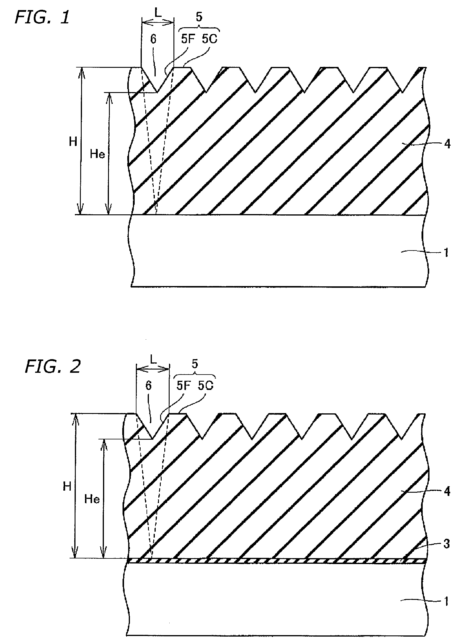
[0041]With reference to FIG. 3, using GaN substrates, which are native substrates, as the growth substrate 1, aperture-window-defining mask layers 2 were formed on the growth substrates, followed by growing GaN crystals 4 over the mask layers 2 by an HVPE technique.

[0042]Each aperture-window-defining mask layer was formed by forming a 100 nm-thick SiO2 layer by CVD, and thereafter forming by photolithography aperture windows that are arrayed in a dotted pattern in which three adjacent aperture windows (squares 2 μm to a side) sit at the vertexes of equilateral triangles (the distance between the adjacent aperture windows being 4 μm).

[0043]By an HVPE technique, GaN crystals were grown to a thickness of about 2 mm on growth substrates at the growth temperatures, GaCl partial pressures, NH3 partial pressures, and growth rates set forth in Table I. Then, the GaN crystals were sliced with a wire saw or an internal-diameter saw and the surfaces were polished to obta...

examples 9 through 12

, Comparative Example 3

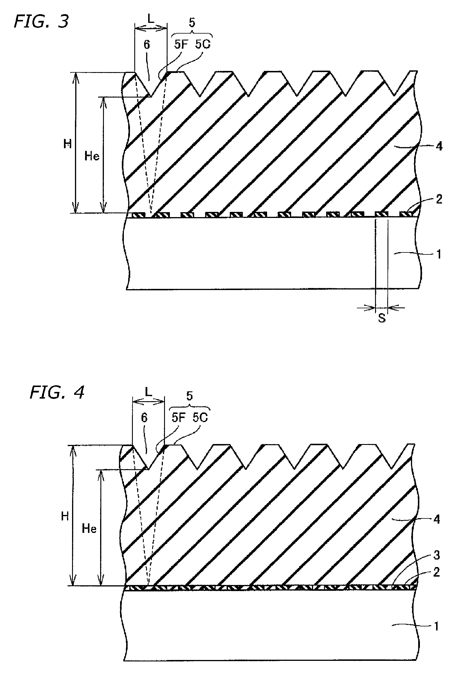
[0045]With reference to FIG. 3, using GaAs substrates, which are foreign substrates, as the growth substrate 1, GaN buffer layers 3 were formed on the growth substrates, followed by growing GaN crystals 4 thereon.

[0046]For the GaN buffer layers 3, amorphous layers having a thickness of about 70 nm were formed, using an HVPE technique, by heating and holding the growth substrate 1 to 500° C. at a GaCl partial pressure of 0.2 kPa and a NH3 partial pressure of 15 kPa.

[0047]With an HVPE technique, GaN crystals were grown to a thickness of about 2 mm over the GaN buffer layers 3 at the growth temperatures, GaCl partial pressures, NH3 partial pressures, and growth rates set forth in Table II. Then, the GaAs substrates were removed by etching in aqua regia, and thereafter the GaN crystals were sliced with a wire saw or an internal-diameter saw and their surfaces polished to obtain GaN crystal substrates having a predetermined thickness. The dislocation densities, pit...


PUM

PropertyMeasurementUnit
crystal-growth temperatureaaaaaaaaaa
partial pressureaaaaaaaaaa

Abstract

Affords a method of manufacturing GaN crystal substrate in which enlargement of pit size in the growing of GaN crystal is inhibited to enable GaN crystal substrate with a high substrate-acquisition rate to be produced. The method of manufacturing GaN crystal substrate includes a step of growing GaN crystal (4) by a vapor growth technique onto a growth substrate (1), the GaN-crystal-substrate manufacturing method being characterized in that in the step of growing the GaN crystal (4), pits (6) that define facet planes (5F) are formed in the crystal-growth surface, and being characterized by having the pit-size increase factor of the pits (6) be 20% or less.

Description

BACKGROUND OF THE INVENTION[0001]1. Field of the Invention[0002]The present invention relates to methods of manufacturing GaN monocrystalline substrates used in light-emitting devices, such as light-emitting diodes (LEDs) and laser diodes (LDs), made from Group III-V semiconductor compounds.[0003]2. Description of the Background Art[0004]As a way of manufacturing large-scale, low-dislocation-density GaN-crystal thick films for application as substrates in LEDs, LDs and other light-emitting devices made from Group III-V semiconductor compounds, one method that has been proposed is, when growing GaN crystal onto a base substrate using a vapor growth technique, to form in the crystal-growth surface pits that define facet planes and to confine the dislocations to, or quench the dislocations along, the boundary lines of the facet planes of the pits, to grow GaN substrates of large area and slight dislocation density. (Cf. Japanese Unexamined Pat. App. Pub. No. 2001-102307, for example.)[...

Claims


Application Information

Patent Timeline
Patent Type & Authority Patents(United States)
IPC IPC(8): C30B23/00C30B29/40C30B29/38H01L21/20H01L21/205H01L21/786H01L27/12
CPCC30B25/02C30B29/406H01L21/786H01L27/12
Inventor OKAHISA, TAKUJI
Owner SUMITOMO ELECTRIC IND LTD
Why Eureka
Try Eureka