Liquid crystal device and electronic apparatus

a liquid crystal device and electronic equipment technology, applied in non-linear optics, instruments, optics, etc., can solve the problems of degrading the display quality at the time of reflective display, which is performed by using light reflected by the reflective display region, and unable to perform vivid display, etc., to achieve vivid display, high-quality display, and high-quality display

Active Publication Date: 2009-01-27
138 EAST LCD ADVANCEMENTS LTD +1
View PDF10 Cites 6 Cited by
  • Summary
  • Abstract
  • Description
  • Claims
  • Application Information

AI Technical Summary

Benefits of technology

[0009]An advantage of some aspects of the invention is that it provides a liquid crystal device in which a film thickness of an insulating layer is changed between a reflective display region and a transmissive display region, such that a thickness of a liquid crystal layer is changed between the two regions. More particularly, an advantage of some aspects of the invention is that it provides a liquid crystal device in which the insulating layer can be provided between adjacent transmissive display regions such that the thickness of the liquid crystal layer is suitably set and an alignment film can be formed so as to have a uniform film thickness among a plurality of transmissive display regions even when the insulating layer is provided between the transmissive display regions.
[0022]Next, according to another aspect of the invention, an electronic apparatus includes the liquid crystal device having the above-described configuration. According to the liquid crystal device of the invention, the function of adjusting the thickness of the liquid crystal layer by use of the insulating layer can be sufficiently achieved, and the alignment film can be formed to have the uniform thickness on the surface of the insulating layer, even when the film thickness of the insulating layer differs between the reflective display region and the transmissive display region. For this reason, according to the liquid crystal device of the aspect of the invention, vivid display can be performed with high display quality. As a result, in the electronic apparatus using the liquid crystal device according to the aspect of the invention, information on the electronic apparatus can be displayed with high display quality. As such an electronic apparatus, for example, a cellular phone, a personal digital assistant, an IC recorder, and other kinds of electronic apparatuses can be considered.

Problems solved by technology

In this case, however, the insulating layer 81 existing among the plurality of transmissive display regions T can get in the way when coating an alignment film 82, so it becomes difficult to uniformly coat the material of the alignment film 82.
In this case, however, although the reflective display region is provided between adjacent transmissive display regions T, the thickness of the liquid crystal layer corresponding to the reflective display region has the large thickness of that used for the transmissive display region, and thus vivid display cannot be performed.
According to this configuration, the insulating layer, which is an obstacle when the material of the alignment film is coated on the insulating layer, is completely removed in that portion.
If any measure is not taken against this problem, display quality at the time of reflective display, which is performed by use of light reflected by the reflective display region, may be degraded.

Method used


Image

  • Liquid crystal device and electronic apparatus
  • Liquid crystal device and electronic apparatus
  • Liquid crystal device and electronic apparatus

Examples


first embodiment

of Liquid Crystal Device

[0042]Hereinafter, a liquid crystal device according to the invention will be described by way of an embodiment. Moreover, it is needless to say that the invention is not limited to the embodiment. Further, in the following description, various structures are exemplified by use of the drawings, but it is necessary to take notice that the structures shown in the drawings have been shown to have different scales from the actual structures such that characteristic portions are easy to understand.

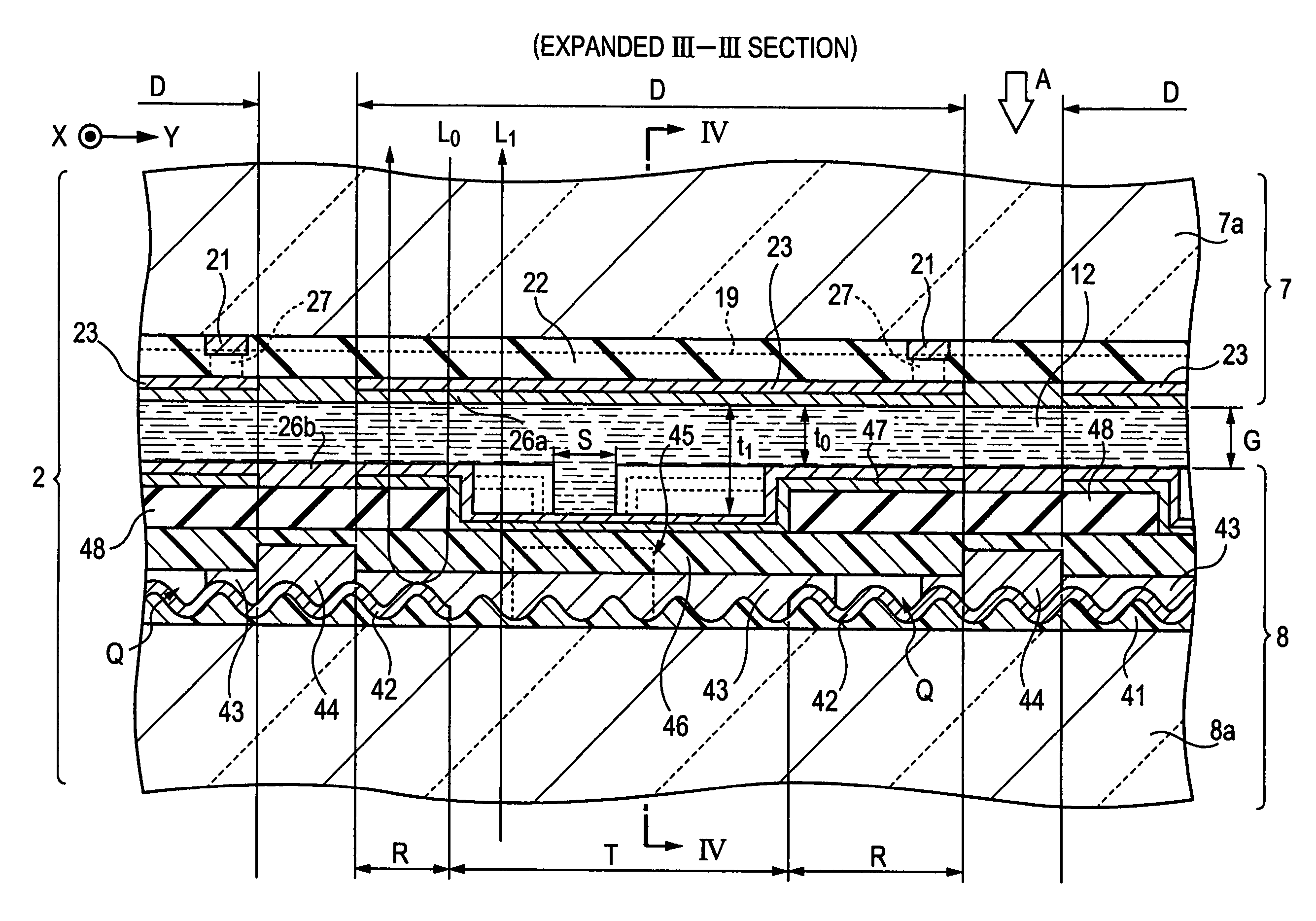
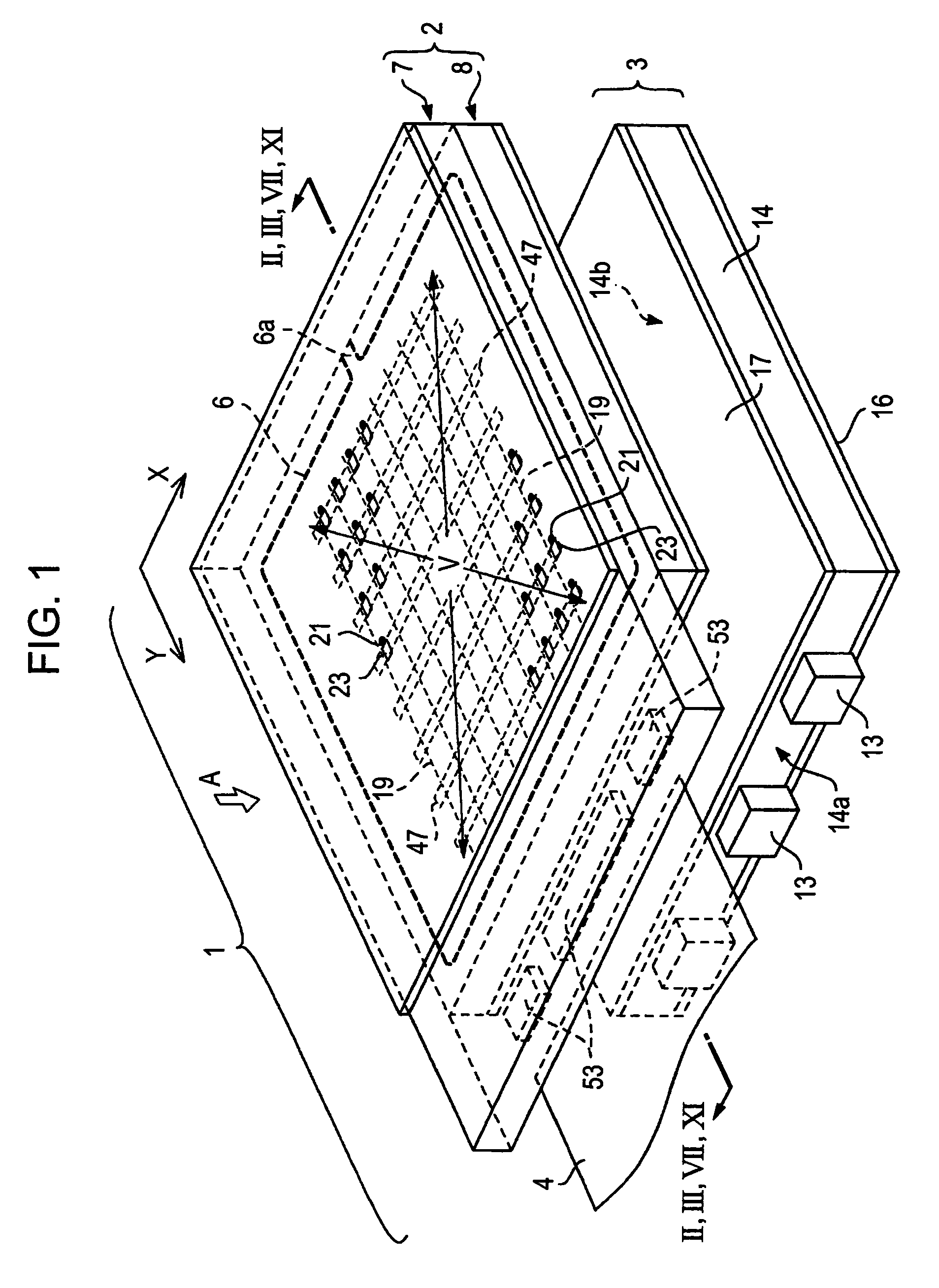
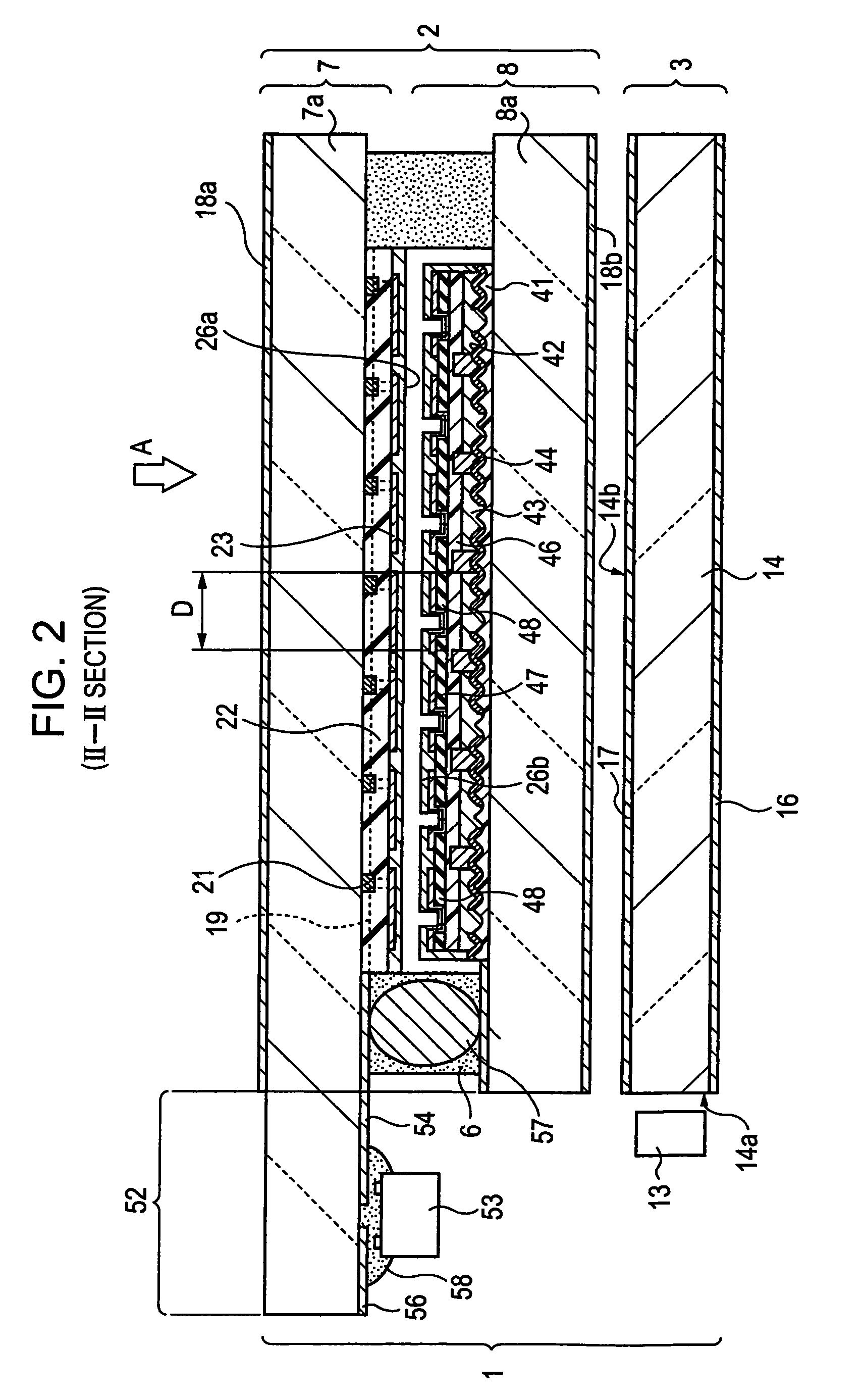
[0043]FIG. 1 shows an embodiment of a liquid crystal device according to the invention. FIG. 2 is a side cross-sectional view taken along the line II-II of FIG. 1. FIG. 3 is a cross-sectional view showing a pixel portion in FIG. 2 on a magnified scale. FIG. 4 is a cross-sectional view taken along the line IV-IV of FIG. 3. FIG. 5 is a plan cross-sectional view taken along the line V-V of FIG. 4. In the present embodiment, the invention is applied to an active matrix-type ...

second embodiment

of Liquid Crystal Device

[0081]FIGS. 7 to 10 show essential parts of another embodiment of a liquid crystal device according to the invention. The overall configuration of the present embodiment can be configured to have the same structure as shown in FIGS. 1 and 2. FIG. 7 is a cross-sectional view showing a pixel portion in FIG. 2 on a magnified scale, like FIG. 3 in the above-described embodiment. Further, FIG. 8 is a cross-sectional view taken along the line VIII-VIII of FIG. 7, like FIG. 4 in the above-described embodiment. Further, FIG. 9 is a plan cross-sectional view taken along the line IX-IX of FIG. 8, like FIG. 5 in the above-described embodiment. Further, FIG. 10 is a diagram showing a laminated state of individual parts on a color filter substrate in exploded view for ease of understanding, like FIG. 6 in the above-described embodiment.

[0082]Hereinafter, the present embodiment will be described, laying emphasis on different parts from those in the first embodiment. In the...

third embodiment

of Liquid Crystal Device

[0087]FIGS. 11 to 14 show essential parts of still another embodiment of a liquid crystal device according to the invention. The present embodiment relates to an active matrix-type liquid crystal device using a TFT (Thin Film Transistor) element, which is a three-terminal-type active element, as a switching element. Moreover, as the TFT element, various kinds of TFTs, such as an amorphous silicon TFT, a low-temperature polysilicon TFT, a high-temperature polysilicon TFT, or the like, may be used. In the present embodiment, it is assumed that the amorphous silicon TFT is used. Of course, the invention can be applied to a liquid crystal device which uses other kinds of TFTs.

[0088]The overall configuration of the present embodiment can be configured to have the same structure as shown in FIG. 1 or 2. FIG. 11 is a cross-sectional view showing a pixel portion in FIG. 2 on a magnified scale, like FIG. 3 in the above-described embodiment. Further, FIG. 12 is a cross...


PUM

PropertyMeasurementUnit
thicknessaaaaaaaaaa
widthaaaaaaaaaa
thickness t2aaaaaaaaaa

Abstract

A liquid crystal device includes a pair of substrates that face each other, a liquid crystal layer that is interposed between the pair of substrates, electrodes that are formed on opposing surfaces of the pair of substrates so as form a plurality of subpixel regions, in each of which a reflective display region having a light-reflective film reflecting light and a transmissive display region transmitting light are provided, and an insulating layer that is formed between one of the pair of substrates and the liquid crystal layer such that a thickness of the liquid crystal layer in the reflective display region is smaller than a thickness of the liquid crystal layer in the transmissive display region. The insulating layer is formed to have a first film thickness in the reflective display region, and is provided between the transmissive display region of a predetermined subpixel region and the transmissive display region of a subpixel region adjacent to the predetermined subpixel region. A portion of the insulating layer is formed to have a film thickness smaller than the first film thickness between the transmissive display region of the predetermined subpixel region and the transmissive display region of the subpixel region adjacent to the predetermined subpixel region.

Description

BACKGROUND[0001]1. Technical Field[0002]The present invention relates to a liquid crystal device in which, in a subpixel region serving as a minimum unit of display, a thickness of a liquid crystal layer is changed in a reflective display region and a transmissive display region. Further, the present invention relates to an electronic apparatus having such a liquid crystal device.[0003]2. Related Art[0004]At present, liquid crystal devices are widely used for electronic apparatuses, such as cellular phones, personal digital assistants, or the like. For example, when various kinds of information on the electronic apparatus are displayed in forms of images, such as characters, numerals, graphics, or the like. In such a liquid crystal device, a plurality of subpixel regions serving as minimum units of display are arranged in a matrix shape in horizontal and vertical directions in a plane of a liquid crystal layer so as to form a display region. Further, by controlling the alignment of ...

Claims


Application Information

Patent Timeline
Patent Type & Authority Patents(United States)
IPC IPC(8): G02F1/1335
CPCG02F1/133555G02F1/136227G02F1/1335G02F1/13
Inventor KAMIJO, KIMITAKAKANEKO, HIDEKIIMAI, KATSUHIRONAKANO, TOMOYUKI
Owner 138 EAST LCD ADVANCEMENTS LTD
Why Eureka
Try Eureka