Semiconductor device temperature sensor and semiconductor storage device

a technology of semiconductor storage and temperature sensor, which is applied in the direction of information storage, static storage, digital storage, etc., can solve the problems of reducing the capacity of a battery and consuming electric power, and achieve the effect of reducing electric power consumption and improving accuracy of temperature detection

Active Publication Date: 2009-02-17
SOCIONEXT INC
View PDF18 Cites 28 Cited by
  • Summary
  • Abstract
  • Description
  • Claims
  • Application Information

AI Technical Summary

Benefits of technology

[0015]An object of the invention is to provide a semiconductor device temperature sensor with the accuracy of temperature detection improved. Further, another object of the invention is to provide a semiconductor storage device, which is arranged by application of a highly accurate temperature sensor so that it can appropriately control the cycle of the refresh action and reduce the electric power consumption.

Problems solved by technology

In other words, with just holding data, a portable system with a DRAM adopted as a memory consumes electric power and decreases the capacity of a battery thereof even when it is not used actually.

Method used


Image

  • Semiconductor device temperature sensor and semiconductor storage device
  • Semiconductor device temperature sensor and semiconductor storage device
  • Semiconductor device temperature sensor and semiconductor storage device

Examples


Embodiment Construction

[0034]Before describing embodiments of a semiconductor device temperature sensor and a semiconductor storage device according to the present invention, a semiconductor device temperature sensor and a semiconductor storage device of a prior art and their associated problems will be described in detail with reference to the accompanying drawings (FIGS. 1 to 12).

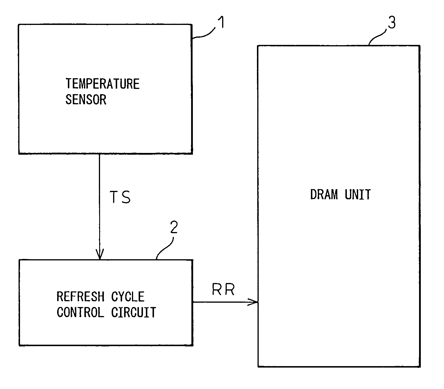
[0035]FIG. 1 is a block diagram conceptually showing an important portion of a DRAM (semiconductor storage device) as an example of a semiconductor device, in which a temperature sensor is applied. In FIG. 1, the reference character 1 shows a temperature sensor, 2 shows a refresh cycle control circuit, and 3 shows a DRAM part.

[0036]The DRAM unit 3 includes a memory unit which needs a refresh action. The temperature sensor 1 detects the temperature of the DRAM unit 3 and outputs a detected temperature signal TS to the refresh cycle control circuit 2. Then, the refresh cycle control circuit 2 outputs a refresh request signal RR t...


PUM


Abstract

A semiconductor device temperature sensor produces a reference level for temperature detection from two or more reference levels of different temperatures to detect a temperature. The temperature sensor is applied for detecting the temperature of a semiconductor storage device having a memory unit which requires a refresh action. A refresh cycle control circuit provided in the semiconductor storage device controls the cycle of the refresh action for the memory unit in response to an output of the temperature sensor.

Description

CROSS-REFERENCE TO RELATED APPLICATION[0001]This application is a continuation application and is based upon PCT / JP04 / 08630, filed on Jun. 18, 2004.BACKGROUND OF THE INVENTION[0002]1. Field of the Invention[0003]The present invention relates to a semiconductor device temperature sensor and a semiconductor storage device and, more particularly, to a temperature sensor for a semiconductor storage device which needs a refresh action in order for a DRAM or the like to hold data.[0004]2. Description of the Related Art[0005]Conventionally, for example, a SRAM (Static Random Access Memory) has been used as a semiconductor storage device (memory) for portable systems including cellular phones. However, the required memory capacity tends to increase with e.g. improvement of the function of portable systems from year to year. Therefore, a DRAM (Dynamic Random Access Memory), which is a memory of large capacity, is going into use as a memory for portable systems. Then, the life time of a batte...

Claims


Application Information

Patent Timeline
Patent Type & Authority Patents(United States)
IPC IPC(8): G11C7/00G11C11/401G11C11/406G11C11/407
CPCG11C7/04G11C11/406G11C11/40626
Inventor SAKO, ATSUMASA
Owner SOCIONEXT INC
Why Eureka
Try Eureka