Strained silicon-on-silicon by wafer bonding and layer transfer

a layer transfer and bonding technology, applied in the direction of semiconductor/solid-state device manufacturing, semiconductor devices, electrical devices, etc., can solve the problems of reducing the thermal conductivity of oxide layers and sisub>1-x/sub>ge/sub>x/sub>layers, increasing the complexity of device fabrication, and forcing process modifications

Inactive Publication Date: 2009-02-24
MASSACHUSETTS INST OF TECH
View PDF24 Cites 3 Cited by
  • Summary
  • Abstract
  • Description
  • Claims
  • Application Information

AI Technical Summary

Benefits of technology

[0008]The invention arises, in part, from the realization that two layers formed of the same semiconducting material, but having different levels of strain, can be bonded directly to one another to maintain a strain in at least one of the layers. Thus, undesirable strain-inducing layers found in prior substrates can be eliminated, while preserving the benefits of utilization of a strained layer. For example, a strained silicon layer can be bonded to an unstrained silicon substrate to eliminate the presence of a Si1-xGex layer and / or an oxide layer in the substrate.

Problems solved by technology

Unfortunately, Si1-xGex-based substrates can increase the complexity of device fabrication.
The presence of the oxide layer, however, forces process modifications.
Further, oxide layers and Si1-xGex layers have reduced thermal conductivity in comparison to conventional silicon wafers.
A reduced thermal conductivity can cause an increase in the difficulty of removing heat at a sufficient rate from devices formed on a substrate.

Method used


Image

  • Strained silicon-on-silicon by wafer bonding and layer transfer
  • Strained silicon-on-silicon by wafer bonding and layer transfer
  • Strained silicon-on-silicon by wafer bonding and layer transfer

Examples


Embodiment Construction

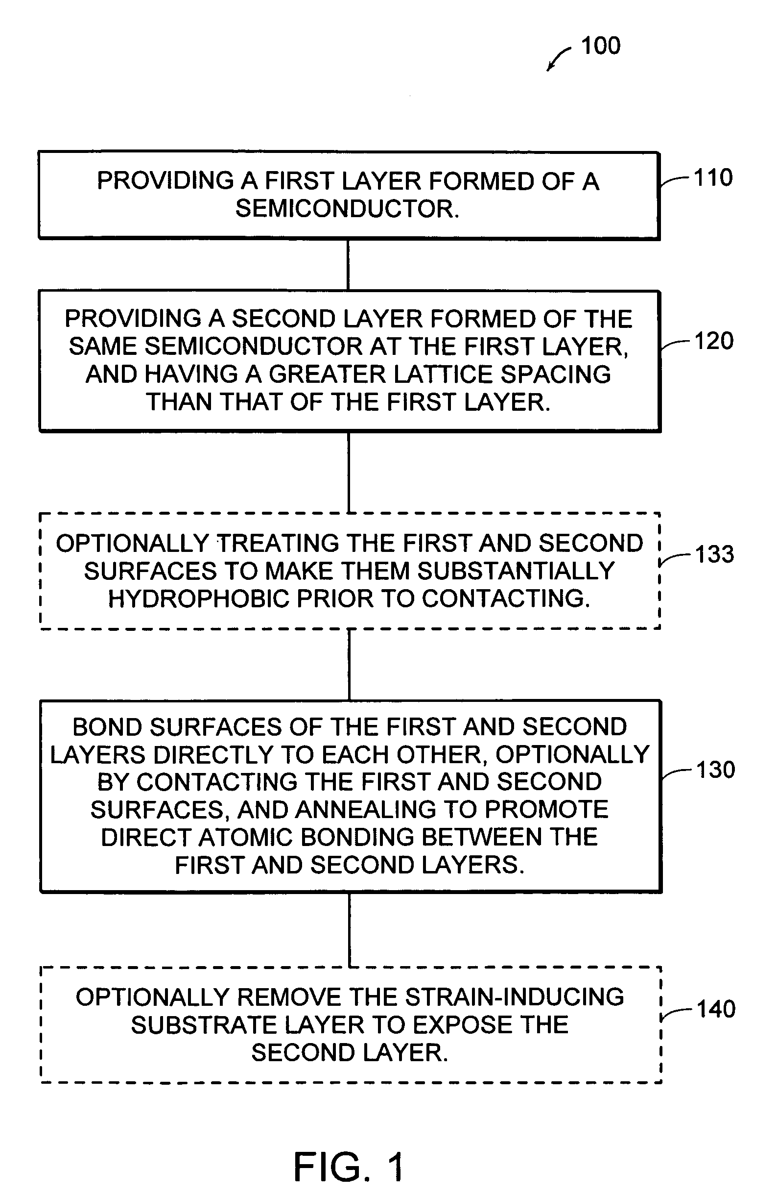
[0018]This invention is not limited in its application to the details of construction and the arrangement of components set forth in the following description or illustrated in the drawings. The invention is capable of other embodiments and of being practiced or of being carried out in various ways. Also, the phraseology and terminology used herein is for the purpose of description and should not be regarded as limiting. The use of “including,”“comprising,” or “having,”“containing,”, “involving,” and variations thereof herein, is meant to encompass the items listed thereafter and equivalents thereof as well as additional items.

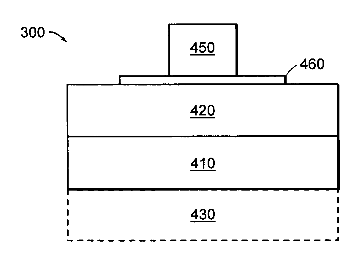
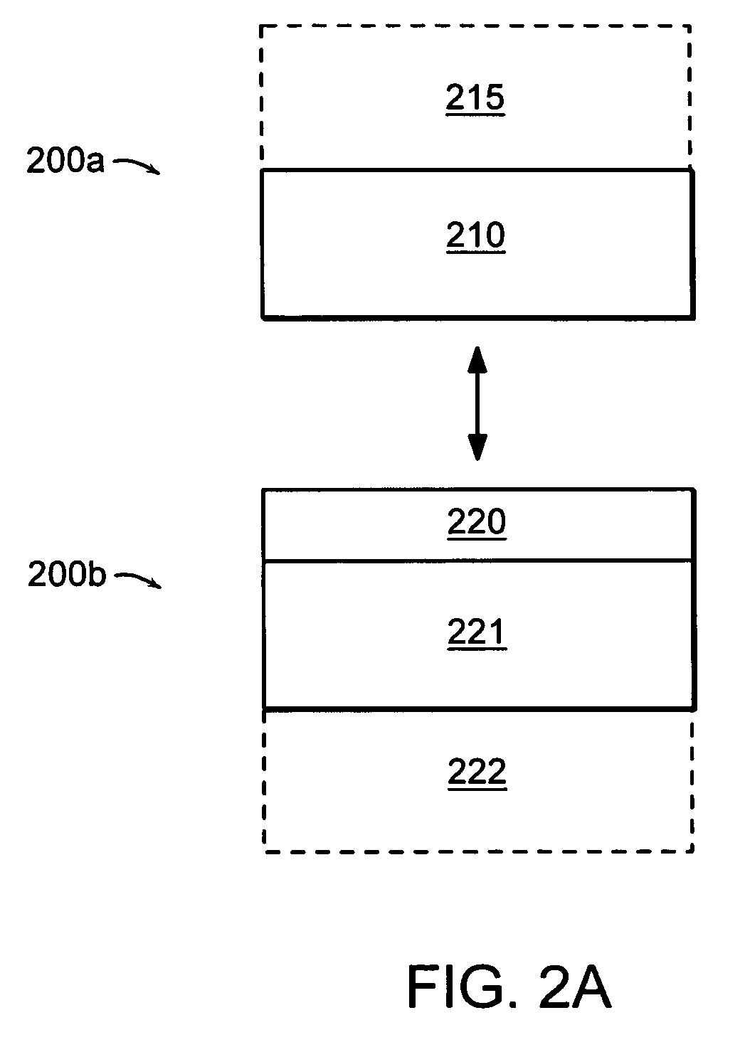
[0019]The term “MOS” is used in this description to refer generally to semiconductor devices that include a conductive gate spaced at least by an insulating layer from a semiconducting channel layer. The terms “SiGe” and “Si1-xGex” are used in this description, depending on context, to interchangeably refer to silicon-germanium alloys. The term “silicide” is u...


PUM


Abstract

A semiconductor-based structure includes first and second layers bonded directly to each other at an interface. Parallel to the interface, the lattice spacing of the second layer is different than the lattice spacing of the first layer. The first and second layers are each formed of essentially the same semiconductor. A method for making a semiconductor-based structure includes providing first and second layers that are formed of essentially the same semiconductor. The first and second layers have, respectively, first and second surfaces. The second layer has a different lattice spacing parallel to the second surface than the lattice spacing of the first layer parallel to the first surface. The method includes contacting the first and second surfaces, and annealing to promote direct atomic bonding between the first and second layers.

Description

BACKGROUND OF INVENTION[0001]1. Field of Invention[0002]The invention relates to semiconductor-based electronic devices, and, more particularly, to the structure and fabrication of semiconductor-based substrates and electronic devices that include strained semiconductor layers.[0003]2. Discussion of Related Art[0004]Some advanced semiconductor-based devices include a semiconductor layer that is strained by application of a stress to provide improved performance of the devices. For example, metal-oxide-semiconductor (MOS) transistors having a channel formed in strained silicon or strained Si1-yGey formed on unstrained, or relaxed, Si1-xGex, can exhibit improved carrier mobility in comparison to traditional p-type MOS (PMOS) and n-type MOS (NMOS) transistors. Strained-layer MOS transistors can be formed on “virtual substrates,” which include a strained layer to provide compatibility with traditional silicon-based fabrication equipment and methods that were designed for use with conven...

Claims


Application Information

Patent Timeline
Patent Type & Authority Patents(United States)
IPC IPC(8): H01L31/0328H01L21/18H01L21/3205
CPCH01L21/187
Inventor ISAACSON, DAVID M.FITZGERALD, EUGENE A.
Owner MASSACHUSETTS INST OF TECH
Why Eureka
Try Eureka