
Insulating buffer film and high dielectric constant semiconductor device and method for fabricating the same

a buffer film and semiconductor technology, applied in the direction of semiconductor devices, basic electric elements, electrical equipment, etc., can solve the problems of increasing the gate leakage current caused by tunnel current coming to the surface, deteriorating carrier mobility, and inability to obtain desired operating current, etc., to achieve enhanced driving performance of transistors

Inactive Publication Date: 2009-02-24
INTERUNIVERSITAIR MICRO ELECTRONICS CENT (IMEC VZW)
View PDF6 Cites 19 Cited by
  • Summary
  • Abstract
  • Description
  • Claims
  • Application Information

AI Technical Summary

Benefits of technology

[0008]It is therefore an object of the present invention to obtain a desired work function by suppressing reaction between a high-κ material and a gate-electrode material that causes Fermi-level pinning so that uniformity and yield are enhanced in a semiconductor device with a CMOS structure, i.e., a dual-gate structure, that is a MOS transistor structure using a fully-silicided gate or a metal gate, and particularly a CMOS semiconductor device using a high-κ material for a gate insulating film.

Problems solved by technology

As the thickness of a gate insulating film decreases in accordance with this size reduction, the problem of increased gate leakage current caused by tunnel current comes to the surface.
In the initial stage of development, the use of a gate insulating film made of metal oxide such as HfO2 or ZrO2 causes a problem in which an interface layer is formed between a silicon substrate and the gate insulating film.
However, once the formation of an interface layer was successfully suppressed so that a high effective relative dielectric constant of the gate insulating film is maintained, i.e., the equivalent oxide thickness EOT is reduced afterward, there arises another problem in which carrier mobility deteriorates as compared to the case of a silicon oxide film and, consequently, desired operating current cannot be obtained.
It has been considered that a cause of this problem is that (1) fixed charge included in a high-κ material electrically interferes with carriers in channel to cause the carrier mobility to deteriorate or (2) carriers in channel are scattered by a lattice in the high-κ material to cause the carrier mobility to deteriorate, for example.
In addition, the use of a high-κ material for a gate insulating film causes another problem.
In addition, regarding this Fermi-level pinning, inversion capacitance of the pMOSFET greatly decreases, which becomes a major obstacle to the use of a high-κ material for a gate insulating film and polysilicon for a gate electrode.
However, for the metal-gate transistor structure, even when a metal having a high melting point is used as a gate-electrode material, a high-temperature process such as activation on source / drain regions is performed, so that Fermi-level pinning occurs and a desired work function is not obtained.
However, this structure has the problem of uneasiness of processes such as gate etching.
However, Fermi-level pinning still occurs in this case, and a desired work function is not obtained.
Moreover, no specific process flows for implementing a CMOS structure are clarified.
299-302), insufficient uniformity and poor yield of a FUSI gate process itself are reported.

Method used


Image

  • Insulating buffer film and high dielectric constant semiconductor device and method for fabricating the same
  • Insulating buffer film and high dielectric constant semiconductor device and method for fabricating the same
  • Insulating buffer film and high dielectric constant semiconductor device and method for fabricating the same

Examples


embodiment 1

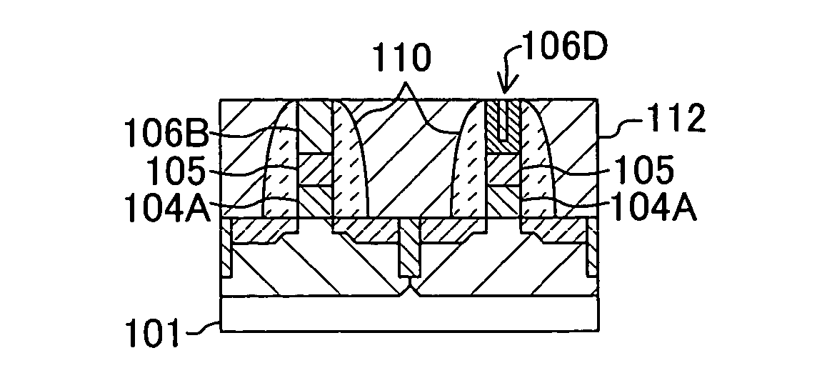
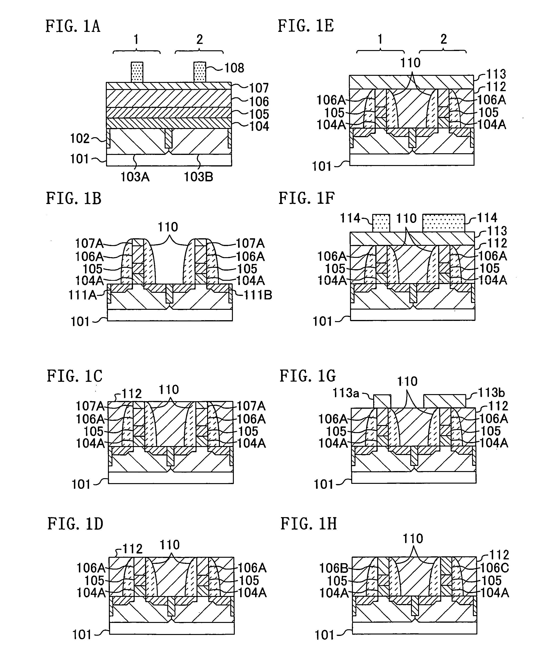
[0081]A method for fabricating a semiconductor device with a CMOS structure according to a first embodiment of the present invention will be described with reference to FIGS. 1A through 1H.

[0082]First, as shown in FIG. 1A, an isolation film 102 serving as a shallow trench isolation (STI) is selectively formed in an upper portion of a substrate 101 made of silicon (Si) having a principal surface whose plane orientation is the (100) plane, for example. Subsequently, ions are implanted in an upper portion of the substrate 101, thereby forming a p-well 103A in an n-transistor region 1 and an n-well 103B in a p-transistor region 2. In this manner, a CMOS device region is formed in the principal surface of the substrate 101. Thereafter, the surface of the substrate 101 is subjected to known standard RCA cleaning and dilute hydrofluoric acid (HF) cleaning in this order. Then, heat treatment is performed on the substrate 101 whose surface has been cleaned, at a temperature of about 600° C. ...

embodiment 2

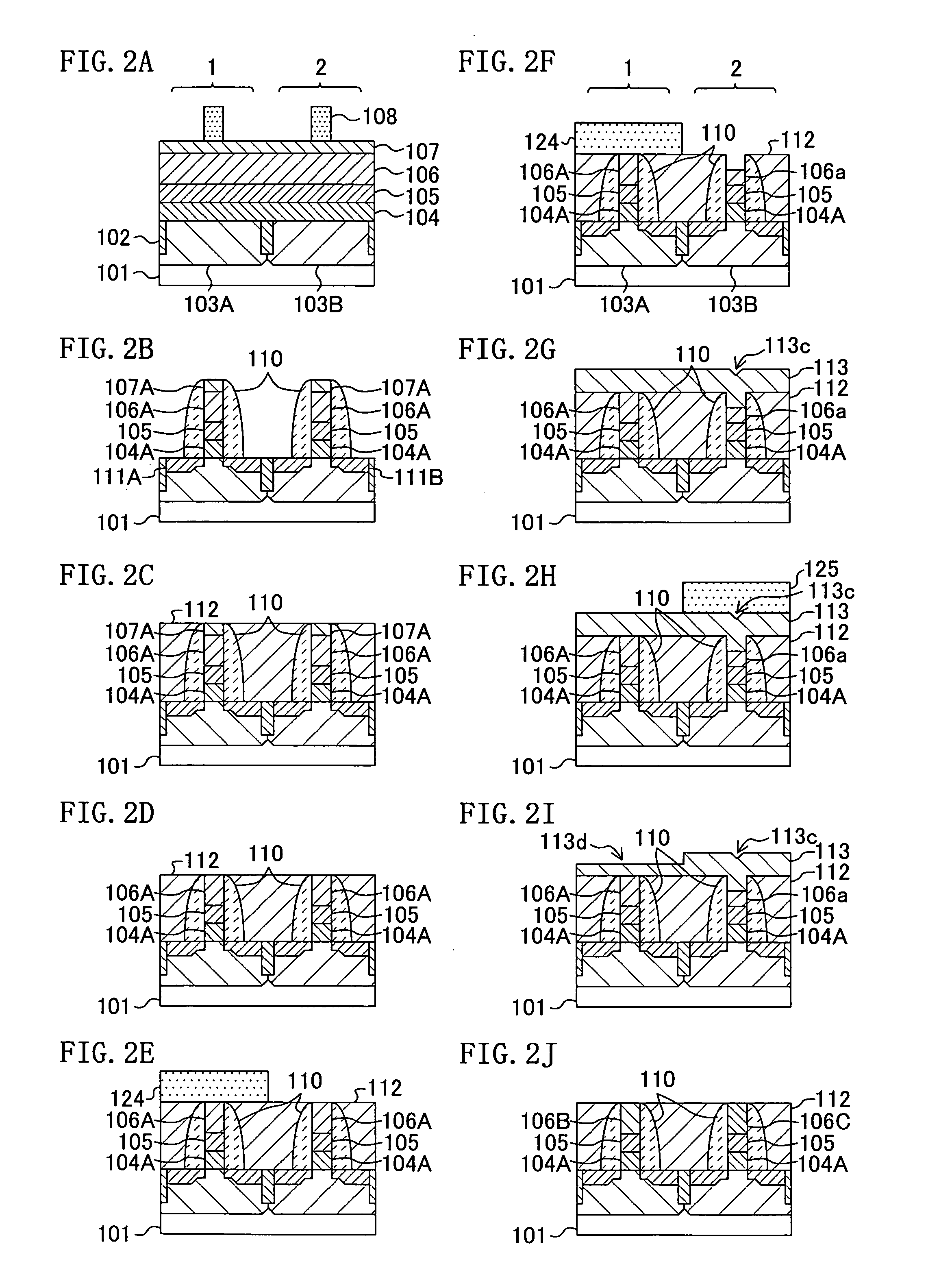
[0102]Hereinafter, a method for fabricating a semiconductor device having a CMOS structure according to a second embodiment of the present invention will be described with reference to FIGS. 2A through 2J. In FIGS. 2A through 2J, components also shown in FIGS. 1A through 1H are denoted by the same reference numerals, and the description thereof will be omitted. The process steps shown in FIGS. 2A through 2D are the same as those described in the first embodiment.

[0103]First, in the process step shown in FIG. 2D, hard masks 107A made of silicon oxide, an upper portion of an interlayer insulating film 112 and upper portions of side walls 110 in an n-transistor region 1 and a p-transistor region 2 are etched back with an etching gas containing fluorocarbon as a main component, thereby exposing gate electrodes 106A.

[0104]Next, as shown in FIG. 2E, a resist pattern 124 is formed on the interlayer insulating film 112 in the n-transistor region 1 or the p-transistor region 2 by lithography...

embodiment 3

[0113]Hereinafter, a method for fabricating a semiconductor device having a CMOS structure according to a third embodiment of the present invention will be described with reference to FIGS. 3A through 3K. In FIGS. 3A through 3K, components also shown in FIGS. 1A through 1H are denoted by the same reference numerals, and the description thereof will be omitted. The process steps shown in FIGS. 3A through 3C are the same as those described in the first embodiment.

[0114]First, as shown in FIG. 3C, an interlayer insulating film 112 made of silicon oxide is deposited over the entire surface of a substrate 101 including hard masks 107A and side walls 110. Subsequently, the upper face of the interlayer insulating film 112 is planarized by, for example, a CMP process, thereby exposing the hard masks 107A.

[0115]Next, as shown in FIG. 3D, a resist pattern 124 is formed on the interlayer insulating film 112 in an n-transistor region 1 or the p-transistor region 2 by lithography to mask the n-t...


PUM


Abstract

A semiconductor device includes: an n-transistor including a first gate insulating film made of a high-dielectric-constant material and a first gate electrode fully silicided with a metal, the first gate insulating film and the first gate electrode being formed in this order over a semiconductor region; and a p-transistor including a second gate insulating film made of the high-dielectric-constant material and a second gate electrode fully silicided with the metal, the second gate insulating film and the second gate electrode being formed in this order over the semiconductor region. If the metal has a work function larger than a Fermi level in potential energy of electrons of silicon, a metal concentration of the second gate electrode is higher than that of the first gate electrode whereas if the metal has a work function smaller than the Fermi level of silicon, a metal concentration of the second gate electrode is lower than that of the first gate electrode.

Description

CROSS-REFERENCE TO RELATED APPLICATION[0001]The disclosure of Japanese Patent Application No. 2005-170208 filed on Jun. 9, 2005 including specification, drawings and claims is incorporated herein by reference in its entirety.BACKGROUND OF THE INVENTION[0002]The present invention relates to methods for fabricating semiconductor devices, and particularly relates to a semiconductor device including a gate insulating film made of a dielectric material having a high dielectric constant (hereinafter, referred to as a high-κ material) and a method for fabricating the device.[0003]With recent increase in the integration degree and speed of semiconductor integrated circuit devices and expansion of the functionality thereof, the size of metal-oxide-semiconductor field effect transistors (MOSFETs) has been reduced. As the thickness of a gate insulating film decreases in accordance with this size reduction, the problem of increased gate leakage current caused by tunnel current comes to the surf...

Claims


Application Information

Patent Timeline
Patent Type & Authority Patents(United States)
IPC IPC(8): H01L29/94
CPCH01L21/28097H01L21/823835H01L21/823842H01L29/513H01L29/517H01L29/66545H01L29/518
Inventor HAYASHI, SHIGENORIMITSUHASHI, RIICHIRO
Owner INTERUNIVERSITAIR MICRO ELECTRONICS CENT (IMEC VZW)
Learn More