Method of developing application-specific integrated circuit devices

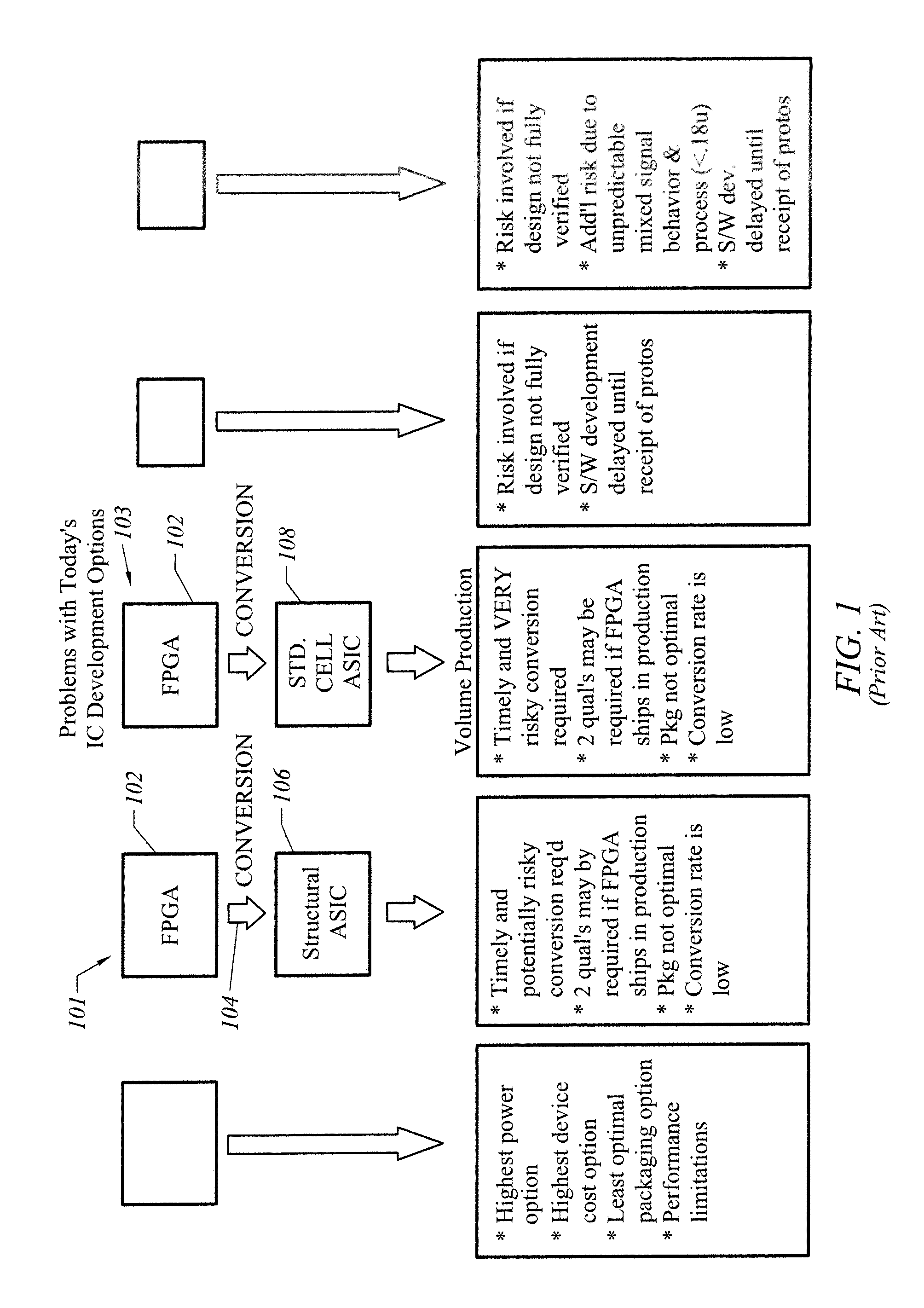
a technology of integrated circuits and integrated circuits, applied in the direction of cad circuit design, program control, instruments, etc., can solve the problems of long design cycle, increased development costs, and extended conversion time to market, and achieve the effect of reducing the amount of time required to produ

Inactive Publication Date: 2009-03-03
SILICON VALLEY BANK
View PDF1 Cites 11 Cited by
  • Summary
  • Abstract
  • Description
  • Claims
  • Application Information

AI Technical Summary

Benefits of technology

[0006]A method, computer readable medium, apparatus and system for developing an Application-Specific Integrated Circuit (“ASIC”) are disclosed. In one embodiment, a method includes defining the functionality of a target ASIC device within a target system, as well as synthesizing circuits for the target ASIC device and a programmable logic device concurrently or nearly concurrently, thereby providing a conversion-less ASIC development flow using one or more programmable devices. In a specific embodiment, the conversion-less ASIC development flow requires no subsequent step of modifying a functional description for the target ASIC device from a functional description expressed in terms of the programmable logic device, thereby reducing an amount of time required to produce the target ASIC device.

Problems solved by technology

A drawback to this traditional design flow is that the conversion extends time-to-market (“TTM”) and increases development costs, among other things. FIG. 1 depicts at least two design flows using conventional FPGA-to-ASIC conversion methodologies.
Both design flows have a drawback of having relatively long design cycles that extends time-to-market.

Method used


Image

  • Method of developing application-specific integrated circuit devices
  • Method of developing application-specific integrated circuit devices
  • Method of developing application-specific integrated circuit devices

Examples


Embodiment Construction

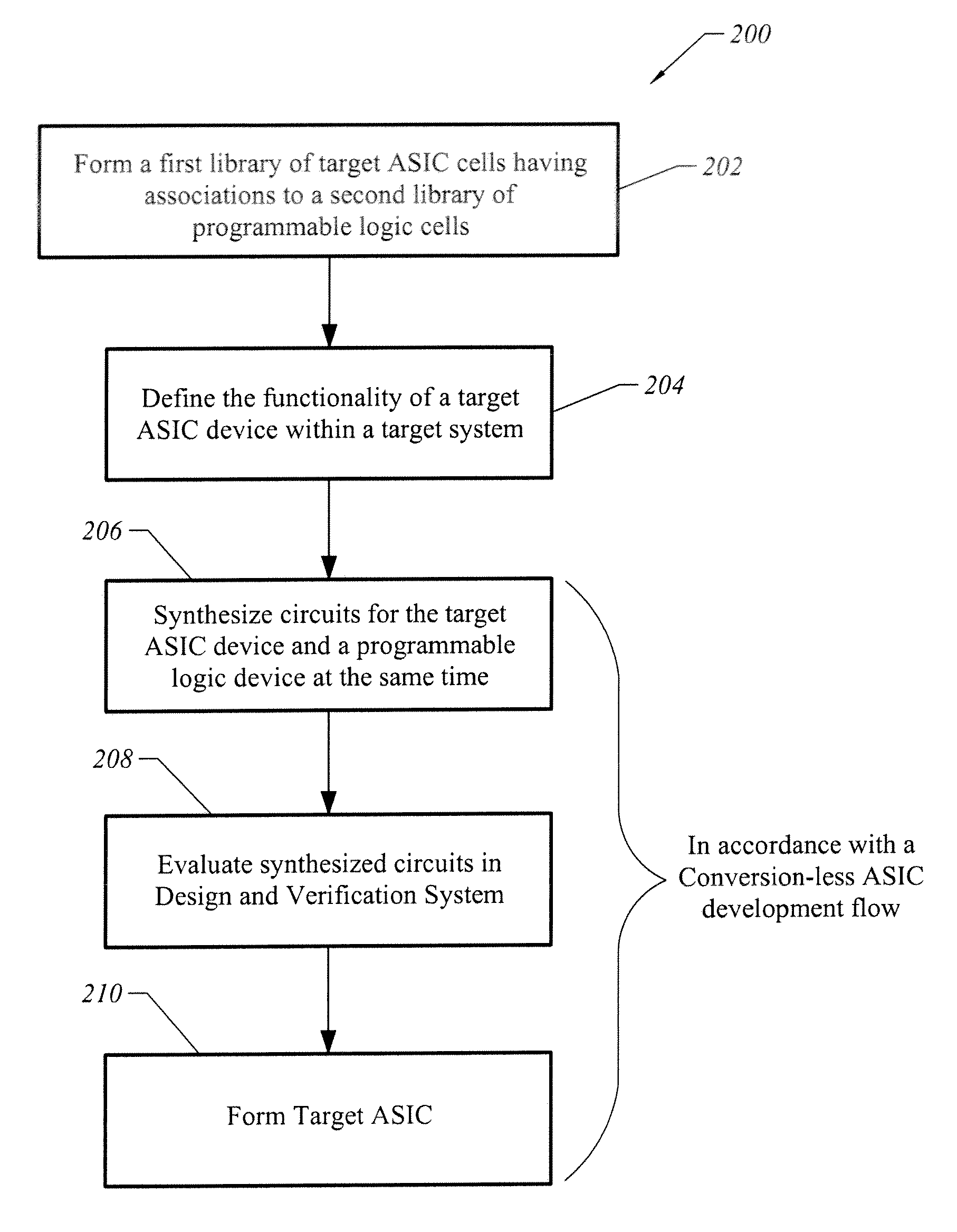
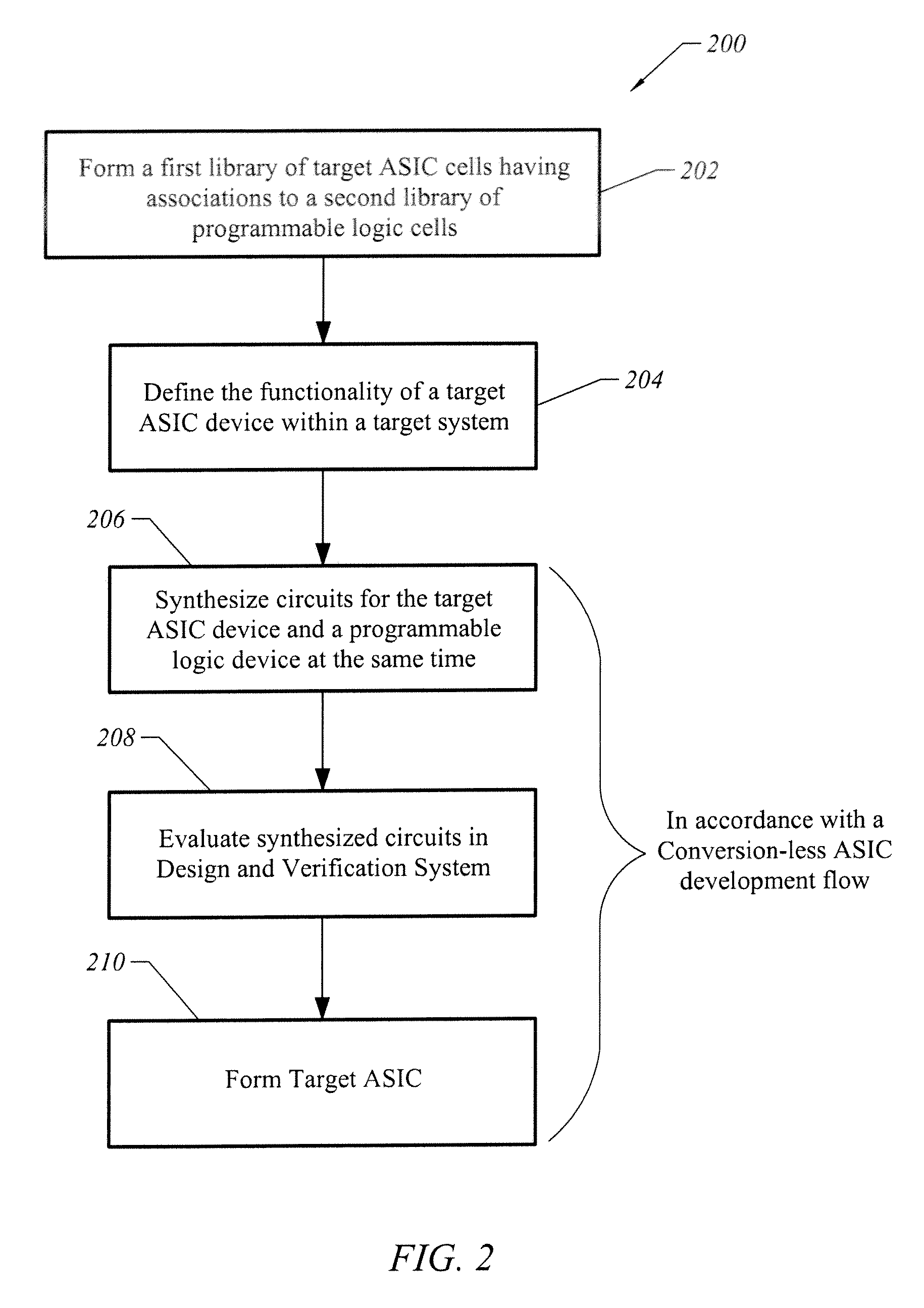
[0015]Various embodiments of the invention provide for design flows and techniques as well as computer readable media for developing ASIC devices. Advantageously, these design flows are conversionless—there is no requirement for an ASIC design cycle for modifying functional descriptions subsequent to a programmable design cycle. That is, there is no need to modify a functional description for a target ASIC device from a functional description that is expressed in terms of a programmable logic device. In a specific embodiment, a single design flow provides for a programmable logic device and an ASIC rather than two separate design flows, which traditionally are performed in series (e.g., a FPGA is first developed in register transfer level (“RTL”), followed by an ASIC design flow that modifies the RTL). In one embodiment, the conversionless approach uses programmable logic device design conventions and techniques (i.e., a programmable logic development flow) to develop an ASIC design...


PUM


Abstract

A method, computer readable medium apparatus and system for developing an Application-Specific Integrated Circuit (“ASIC”) are disclosed. In one embodiment, a method includes defining the functionality of a target ASIC device within a target system, as well as synthesizing circuits for the target ASIC device and a programmable logic device concurrently or nearly concurrently, thereby providing a conversion-less ASIC development flow using one or more programmable devices. In a specific embodiment, the conversion-less ASIC development flow requires no subsequent step of modifying a functional description for the target ASIC device from a functional description expressed in terms of the programmable logic device, thereby reducing an amount of time required to produce the target ASIC device.

Description

CROSS REFERENCE TO RELATED APPLICATIONS[0001]This application claims the benefit of U.S. Provisional Application Ser. No. 60 / 720,258, entitled “Conversionless Development Of Application-Specific Integrated Circuit (“ASIC”) Devices,” filed Sep. 23, 2005, the contents of which are hereby incorporated by reference in their entirety.BRIEF DESCRIPTION OF THE INVENTION[0002]This invention relates generally to circuit design and development, and more particularly, to developing an application-specific integrated circuit (“ASIC”) while foregoing a conversion, for example, from a Field-Programmable Gate Array (“FPGA”) prototype or any other type of programmable logic device to an ASIC device.BACKGROUND OF THE INVENTION[0003]A traditional design flow for developing ASICs, including standard cell-based ASICs, structured ASICs and other similar types of ASICs, includes a conversion from an FPGA design to an ASIC design. An FPGA-to-ASIC conversion methodology typically employs an FPGA for protot...

Claims


Application Information

Patent Timeline
Patent Type & Authority Patents(United States)
IPC IPC(8): G06F17/50
CPCG06F17/5045G06F30/30
Inventor MASSABKI, ELIE H.AMARILIO, LIOR
Owner SILICON VALLEY BANK
Why Eureka
Try Eureka