Organic light emitting display

a light-emitting display and organic technology, applied in the direction of luminescnet screens, identification means, instruments, etc., can solve the problems of deterioration of reducing the emission region, and reducing the efficiency of organic light-emitting, so as to improve the organic light-emitting display

Active Publication Date: 2009-03-10
SAMSUNG DISPLAY CO LTD
View PDF12 Cites 22 Cited by
  • Summary
  • Abstract
  • Description
  • Claims
  • Application Information

AI Technical Summary

Benefits of technology

[0020]It is, therefore, an object of the present invention to provide an improved organic light emitting display.
[0021]It is also an object of the present invention to provide an organic light emitting display that has a structure with a reduced step height and a reduced taper angle of a pixel defining layer to prevent device failure from occurring in an organic emission layer.

Problems solved by technology

Further, since the organic emission layer is not uniformly deposited around the first hole and the second hole and at the stepped region of the anode, there were problems that a dark spot was generated by a concentrated phenomenon of current density when a voltage between the anode and the cathode was applied, and that an emission region was reduced due to the generation of the dark spot to degrade picture quality.
When the characteristics of the emission layer are changed, there were problems of characteristic deterioration, such as the deterioration of the efficiency of the resultant organic light emitting display, a change in the color coordinate, and reduction of the life-time.
That is, when the organic emission layer is not rightly transferred or even when it is regularly transferred, a defect such as unclean transfer boundary is generated.

Method used


Image

  • Organic light emitting display
  • Organic light emitting display
  • Organic light emitting display

Examples


first embodiment

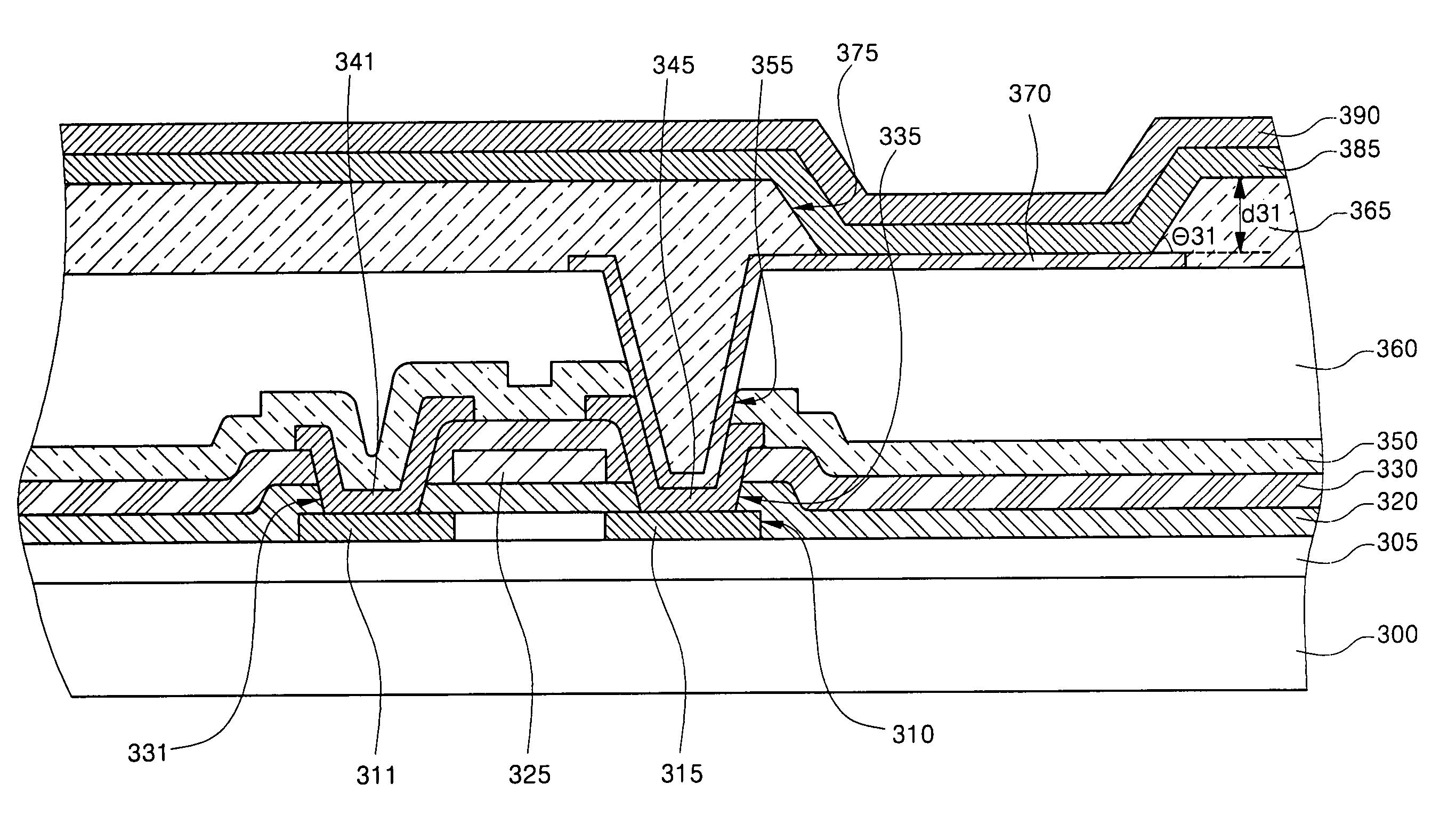
[0043]FIG. 7 is a cross-sectional view of a top-emission organic light emitting display according to the present invention. Referring to FIG. 7, a buffer layer 305 is formed on an insulating substrate 300, and a semiconductor layer 310 having source / drain regions 311, 315 is formed on the buffer layer 305. A gate electrode 325 is formed on a gate insulating layer 320, and source / drain electrodes 341, 345 connected to the source / drain regions 311, 315 through first holes 331, 335 are formed in an interlayer insulating layer 330.

[0044]A planarization layer 360 is formed on a passivation layer 350, and an anode 370, which is a lower electrode connected to one of the source / drain electrodes 341, 345, for example, the drain electrode 345, through a second hole 355, is formed in the planarization layer 360. A pixel defining layer 365 including an opening 375 that exposes a portion of the anode 370 is formed on the planarization layer, and an organic thin film layer 385 and a cathode 390 a...

second embodiment

[0058]FIG. 8 is a cross-sectional view illustrating a top-emission organic light emitting display according to the present invention. Referring to FIG. 8, a buffer layer 405 is formed on an insulating substrate 400, and a semiconductor layer 410 including source / drain regions 411, 415 are formed on the buffer layer 405. A gate electrode 425 is formed on a gate insulating layer 420, and source / drain electrodes connected to the source / drain regions 411, 415 are formed in an interlayer insulating layer 430 through first holes 431, 435.

[0059]A planarization layer 460 is formed on a passivation layer 450, and an anode 470, which is a lower electrode connected to one of the source / drain electrodes 441, 445, for example, the drain electrode 445 through a second hole 455, is formed in the planarization layer 460. An organic thin film layer 485 and a cathode 490 are formed on the TFT substrate. The organic thin film layer 485 includes at least an emission layer selected from a hole injection...

third embodiment

[0061]FIG. 9 is a cross-sectional view illustrating a bottom-emission organic light emitting display according to the present invention. Referring to FIG. 9, a buffer layer 505 is formed on an insulating substrate 500, and a semiconductor layer 510 including source / drain regions 511, 515 are formed on the buffer layer 505. A gate electrode 525 is formed on a gate insulating layer 520, and source / drain electrodes 541, 545 is formed in an interlayer insulating layer 530 through first holes 531, 535.

[0062]An anode 570, which is a lower electrode connected to one of the source / drain electrodes 541, 545, for example, the drain electrode 545, through a second hole 555, is formed in a passivation layer 550. A pixel defining layer 565 including an opening 575 that exposes a portion of the anode 570 is formed, and an organic thin film layer and a cathode 590, an upper electrode, are formed on the pixel defining layer 565 and the anode 570 of the opening 575. The organic thin film layer 585 i...


PUM


Abstract

An organic light emitting display which is constructed with a TFT substrate having an insulating substrate and a TFT that has at least a source electrode and a drain electrode, a lower electrode formed on the TFT substrate and connected to one of source / drain electrodes, an insulating layer having an opening that exposes a portion of the lower electrode, an organic thin film layer formed on the exposed portion of the lower electrode and the insulating layer, and an upper electrode formed on the organic thin film layer, wherein the insulating layer has a taper angle less than 40° at an edge of the opening, and a step less than or equal to 3,000 Å is formed between the lower electrode and the organic thin film layer. The organic light emitting display can prevent device failure.

Description

CLAIM OF PRIORITY[0001]This application makes reference to, incorporates the same herein, and claims all benefits accruing under 35 U.S.C. §119 from an application for ORGANIC LIGHT EMITTING DISPLAY earlier filed in the Korean Intellectual Property Office on 29 Nov. 2003 and there duly assigned Serial No. 2003-87789.BACKGROUND OF THE INVENTION[0002]1. Field of the Invention[0003]The present invention relates to an organic light emitting display and, more particularly, to a full color active matrix organic light emitting display that can reduce a step height between an organic thin film layer and a lower electrode and relieve a taper angle of a substrate surface to prevent device failure from occurring.[0004]2. Description of the Related Art[0005]Generally, an active matrix organic light emitting display (AMOLED) has a structure such that a thin film transistor (TFT) is arranged on a substrate in a form of a matrix, an anode connected to the TFT is formed, and an organic thin film la...

Claims


Application Information

Patent Timeline
Patent Type & Authority Patents(United States)
IPC IPC(8): H01J63/04G09F9/30H01L51/50H01L27/32H05B33/22
CPCH01L27/3246H01L27/3258H01L51/5206H01L51/5221H01L27/1248H01L51/0013H01L2251/5315H01L2251/5323H01L2251/558H10K59/122H10K59/123H10K59/124H10K71/18H10K2102/3026H10K2102/3031H10K2102/351H10K59/8052H10K59/8051H10K59/80515H10K59/80521H05B33/22H10K50/81H10K50/82
Inventor KIM, MU-HYUNSONG, MYUNG-WONKANG, TAE-MINLEE, SEONG-TAEKCHO, YU-SUNG
Owner SAMSUNG DISPLAY CO LTD
Why Eureka
Try Eureka