Method and circuit for the detection of solder-joint failures in a digital electronic package

a digital electronic package and solder joint technology, applied in the direction of individual semiconductor device testing, semiconductor/solid-state device testing/measurement, instruments, etc., can solve the problems of reduced reliability, solder-joint connection from digital electronic package such as fpgas or microcontroller to printed wire board (pwb) is a major reliability problem, and reduces reliability. , the effect of manufacturing defects and electronic package operation

Inactive Publication Date: 2009-03-10
RIDGETOP GROUP
View PDF15 Cites 27 Cited by
  • Summary
  • Abstract
  • Description
  • Claims
  • Application Information

AI Technical Summary

Problems solved by technology

Solder-joint connections from digital electronic packages such as FPGAs or Microcontrollers to Printed Wire Boards (PWB) are a major reliability problem.
The increased number of pins on the packages is necessary to support the evolving complexity of circuits; however, one of the drawbacks of the increase is reduced reliability.
Failure mechanisms include manufacturing defects and operation of the electronic package.
Manufacturing defects may include variance in the materials, variance in the manufacturing process or assembly of one specific package.
These types of defects will produce a high probability of failure early in the expected life cycle of a part.
These stresses will typically produce random failures at a fairly low rate during the useful life of the period; then near the end of the expected life cycle the failure rate will increase due to accumulated fatigue of the solder joints.
Although failures typically occur at the interface of a BLM and its attached ball or at the interface of a PWB LAND and its attached ball, the same failure mechanisms might cause solder joint failures within the package itself at any of the connections.
Any such failure will result in a defective electronic package.
They conclude that solder-joint networks fail intermittently and as hard failures.
An intermittent failure manifests itself during thermal or mechanical transients or disturbances in the form of short-duration high-resistance spikes.
The second type of solder-joint failure is a hard failure, which manifests itself as a steady-state high-impedance, including an open of infinite impedance.
If a number of devices fail initially or early on then there may be something wrong with the materials or process control.
None of these tests are suitable for testing actual fielded devices during operation.
The techniques for direct measurement of the solder-joint resistance have a number of limitations.
It follows that these tests cannot be performed on actual operational devices, either in the lab or particularly in the field.
Finally, there are several instruments available to perform these measurements, however, besides being bulky and suitable for lab testing, these instruments cannot be used to perform real-time, in-use testing of fielded, operational FPGA BCA solder joint networks.
The current test procedures for measuring the resistance may be adequate for evaluating the condition of the solder joints formed by the primary BGA during or after the various stress tests to evaluate the design or potential manufacturing defects, but they are not applicable to actual operational devices, particularly for ongoing testing during the normal operation of a fielded device.
Furthermore, these tests are not capable of evaluating the internal solder-joint connections of the FPGA BGA package or the flip-chip prior to subsequent assembly and fielding of the device.

Method used


Image

  • Method and circuit for the detection of solder-joint failures in a digital electronic package
  • Method and circuit for the detection of solder-joint failures in a digital electronic package
  • Method and circuit for the detection of solder-joint failures in a digital electronic package

Examples


Embodiment Construction

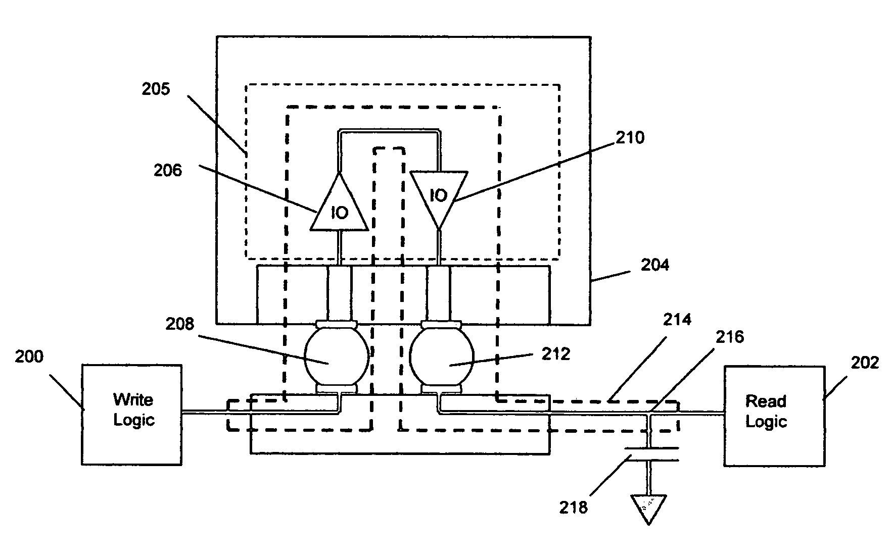
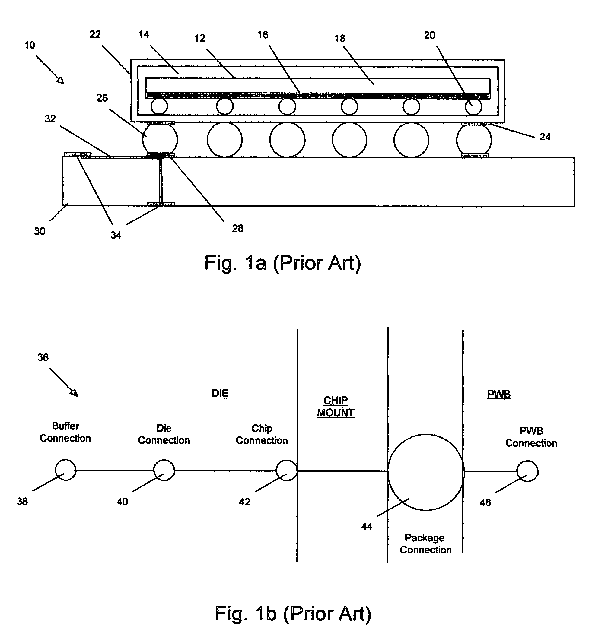
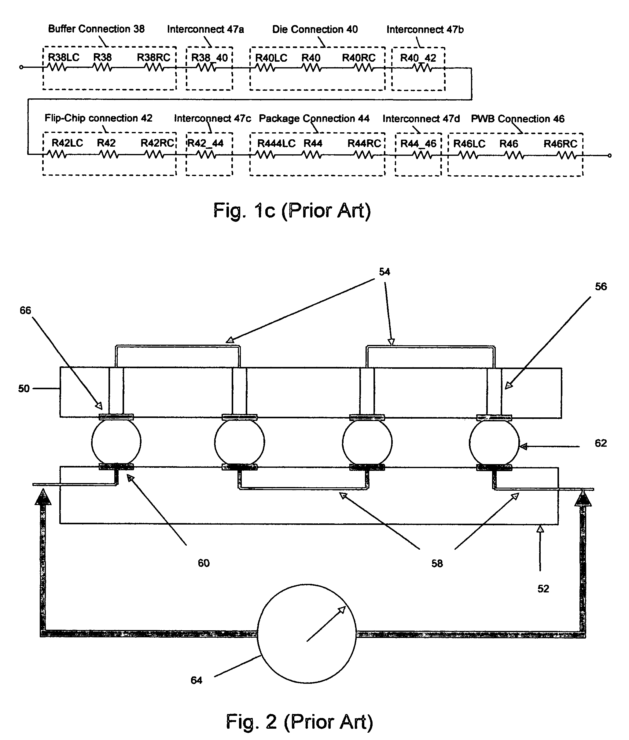
[0054]The present invention provides a method for evaluating solder-joint integrity of operational digital electronic packages, such as FPGAs or Microcontrollers that have internally connected input / output (I / O) buffers and high density ball grid array packages, and particularly for evaluating the integrity of the solder-joint network during normal operation of the digital electronic packages. The invention will be described for a FPGA including a flip-chip mounted in a BGA package that is reflow soldered to a PWB, but it will be understood that the method and circuit for evaluating solder-joint integrity is generally applicable to any digital electronic package that has internally connected input / output buffers in the solder-joint network regardless of whether the die is configured as an FPGA, microcontroller or otherwise, or whether a specific mount method, such as a flip-chip is used, or whether a specific bonding method, such as wire bonding is used, or regardless of a specific ...


PUM


Abstract

The solder-joint integrity of digital electronic packages, such as FPGAs or microcontrollers that have internally connected input / output buffers, is evaluated by applying a time-varying voltage through one or more solder-joint networks to charge a charge-storage component. Each network includes an I / O buffer on the die in the package and a solder-joint connection, typically one or more such connections inside the package and between the package and a board. The time constant for charging the component is proportional to the resistance of the solder-joint network, hence the voltage across the charge-storage component is a measurement of the integrity of the solder-joint network.

Description

CROSS-REFERENCE TO RELATED APPLICATIONS[0001]This application claims benefit of priority under 35 U.S.C. 119(e) to U.S. Provisional Application No. 60 / 657,101 entitled “Non-Invasive Real Time Method for the Detection of Solder Joint Failures” filed on Feb. 28, 2005, the entire contents of which are incorporated by reference.GOVERNMENTAL RIGHTS[0002]This invention was made with Government support under Contract N68335-05-C-0101 awarded by Naval Air Warfare Center AD (LKE). The Government has certain rights in this invention.BACKGROUND OF THE INVENTION[0003]1. Field of the Invention[0004]This invention relates to a method and circuit for detection of solder joint failures in digital electronic packages such as Field Programmable Gate Arrays (FPGAs) and Microcontrollers and between the packages's ball grid array (BGA) and printed wire board (PWB).[0005]2. Description of the Related Art[0006]Solder-joint connections from digital electronic packages such as FPGAs or Microcontrollers to P...

Claims


Application Information

Patent Timeline
Patent Type & Authority Patents(United States)
IPC IPC(8): G01R31/02
CPCG01R31/048G01R31/2884G01R31/312G01R31/71
Inventor SPUHLER, PHILIPP S.VERMEIRE, BERT M.HOFMEISTER, JAMES P.
Owner RIDGETOP GROUP
Why Eureka
Try Eureka