Methods and apparatus for inline measurement of switching delay history effects in PD-SOI technology

a technology of switching delay and history effect, applied in the field of integrated circuit device inline techniques for measuring the history effect of switching delay in the integrated circuit device, can solve the problems of difficult processing of measurements, failure to correlate this history with ss delays,

Inactive Publication Date: 2009-03-17
IBM CORP
View PDF5 Cites 6 Cited by
  • Summary
  • Abstract
  • Description
  • Claims
  • Application Information

AI Technical Summary

Benefits of technology

[0007]The present invention provides techniques for inline measurement of switching delay history effects with respect to steady state delay in PD-SOI technology.

Problems solved by technology

These measurements are difficult to perform during processing in a manufacturing environment because of problems with noise, shielding and test time.
Measuring only the 1SW-2SW history provides considerable insight in the delay variability, but also fails to correlate this history with SS delays.

Method used


Image

  • Methods and apparatus for inline measurement of switching delay history effects in PD-SOI technology
  • Methods and apparatus for inline measurement of switching delay history effects in PD-SOI technology
  • Methods and apparatus for inline measurement of switching delay history effects in PD-SOI technology

Examples


Embodiment Construction

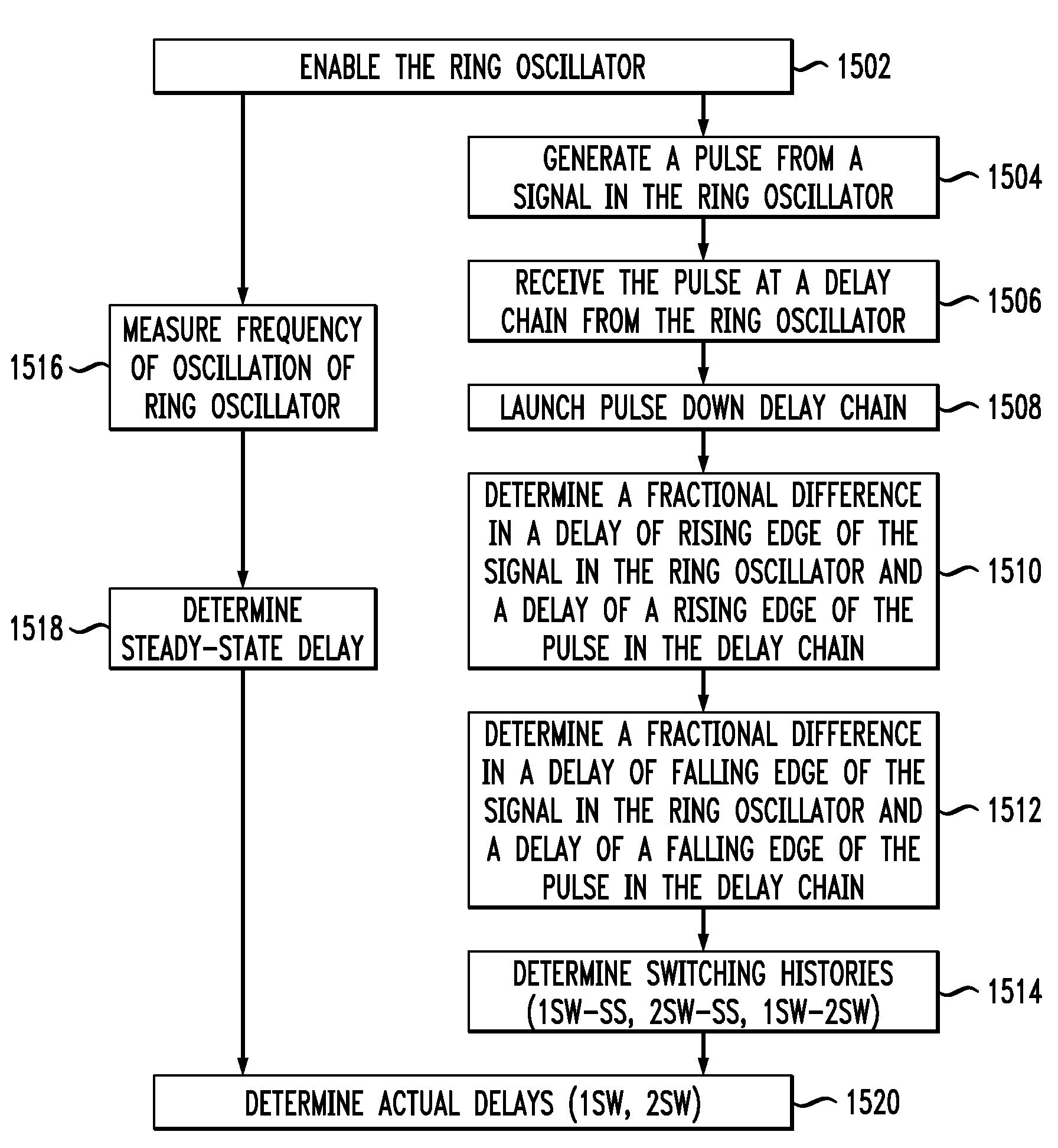
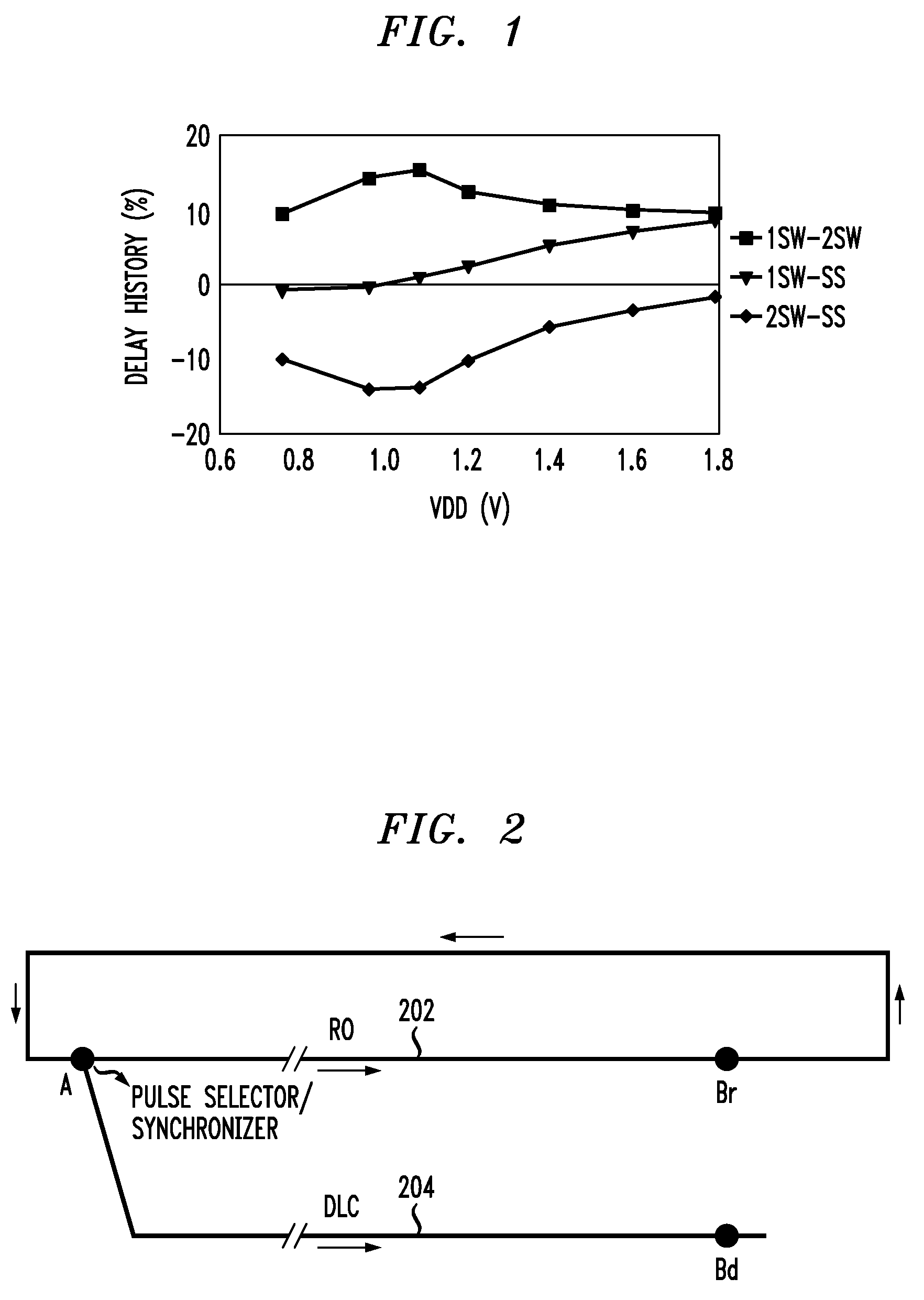
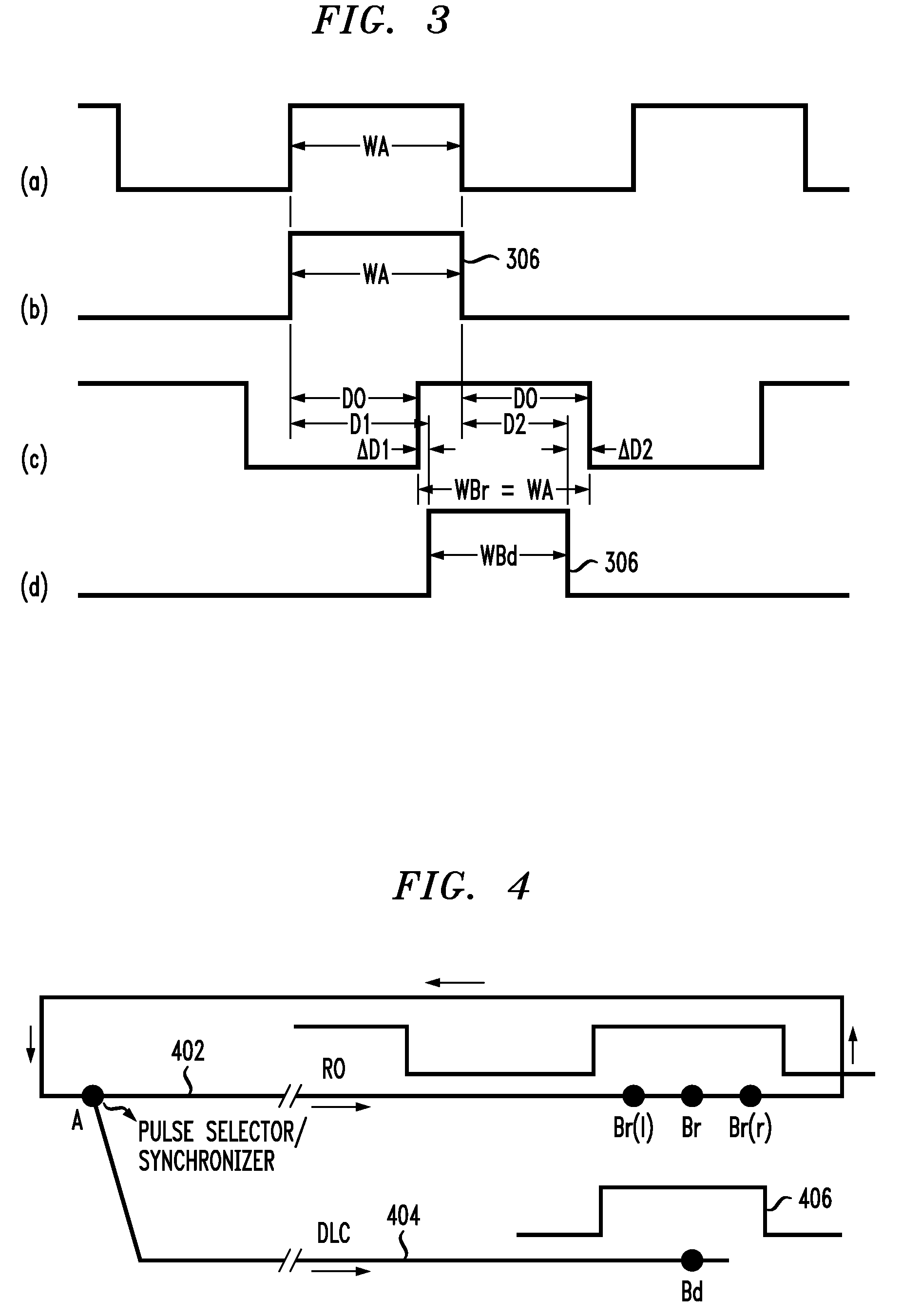
[0030]An integrated circuit device is provided for measuring the 1SW-SS, 2SW-SS 1SW-2SW history in CMOS gates fabricated in PD-SOI technology. The embodiments of the present invention perform measurements independent of the relative magnitudes of 1SW, 2SW and SS delays. Such embodiments consist of a ring oscillator (RO), with a period of oscillation of a few ns, a delay chain (DLC), a circuit to launch a pulse down the DLC synchronously with the signal of the RO, and a circuit to measure the position of the rising and falling edges of the pulse with respect to corresponding edges of the signal of the RO. Both the difference in 1SW and 2SW delays with respect to SS delay and the absolute magnitudes of these delays are determined in units of the delay of the inverting CMOS gate utilized in the RO and DLC. The SS gate delay is extracted from the frequency of oscillation of the RO which after dividing down to a few MHz can be easily measured with an off-the-shelf frequency counter, see,...


PUM


Abstract

Techniques for inline measurement of switching delay history effects in an integrated circuit device are provided. A pulse is launched down a delay chain. The pulse is substantially synchronized with a signal of a ring oscillator. The delay chain and the ring oscillator comprise substantially identical gates to a defined point on the ring oscillator corresponding to a far end of the delay chain. At least one difference in a number of gates traversed by an edge of the signal in the ring oscillator and a number of gates traversed by a corresponding edge of the pulse in the delay chain is measured when the pulse reaches the far end of the delay chain. One or more switching histories in the integrated circuit device are determined in accordance with the at least one measured difference in the number of gates traversed by an edge of the signal and a corresponding edge of the pulse.

Description

FIELD OF THE INVENTION[0001]The present invention relates generally to integrated circuit devices and, more particularly, to inline techniques for measurement of switching delay history effects in an integrated circuit device.BACKGROUND OF THE INVENTION[0002]In a complementary metal-oxide semiconductor (CMOS) circuit in partially depleted silicon on insulator (PD-SOI) technology, the delay is dependent on its switching history. When a circuit first switches after sitting idle for a few milliseconds (ms) or more it will have a longer or shorter delay than when it switches again within a few nanoseconds (ns). The first switch of the circuit is referred to herein as 1SW, while the second switch is referred herein as 2SW. If the same circuit is switching on a regular basis, every few ns or less, it will have a third delay characteristic of steady state operation, referred to herein as SS. These effects, known as SOI history, are required to be measured to accurately characterize the per...

Claims


Application Information

Patent Timeline
Patent Type & Authority Patents(United States)
IPC IPC(8): H03K3/03G01R23/175G01R29/02
CPCH03K3/0315
Inventor BHUSHAN, MANJULKETCHEN, MARK B.
Owner IBM CORP
Why Eureka
Try Eureka