Reference supply voltage circuit using more than two reference supply voltages

a supply voltage and reference supply technology, applied in the direction of automatic control, process and machine control, instruments, etc., can solve the problems of increasing the size of the circuit, unsuitable for a reduction in size, and the difference between the threshold voltages of the circuit elements in both internal circuits, so as to achieve the effect of reducing the siz

Inactive Publication Date: 2009-03-24
PANASONIC CORP
View PDF3 Cites 2 Cited by
  • Summary
  • Abstract
  • Description
  • Claims
  • Application Information

AI Technical Summary

Benefits of technology

[0006]An essential object of the present invention is to solve the aforementioned problems, and to provide a reference supply voltage circuit which is safe and suitable for reduction in size even when a high reference supply voltage is used in a reference supply voltage circuit having more than two reference supply voltages.

Problems solved by technology

However, in the semiconductor device for the switching power supply of the prior art, in the case where a high supply voltage (for example, equal to or higher than 15V) is required, there is such a problem that the circuit size increases and becomes unsuitable for a reduction in size because a plurality of high withstand voltage circuit elements are required.
However, in this case, a difference between threshold voltages of the circuit elements in both internal circuits increases, and this may lead to a false operation of the whole circuit.

Method used


Image

  • Reference supply voltage circuit using more than two reference supply voltages
  • Reference supply voltage circuit using more than two reference supply voltages
  • Reference supply voltage circuit using more than two reference supply voltages

Examples


embodiment 1

Preferred Embodiment 1

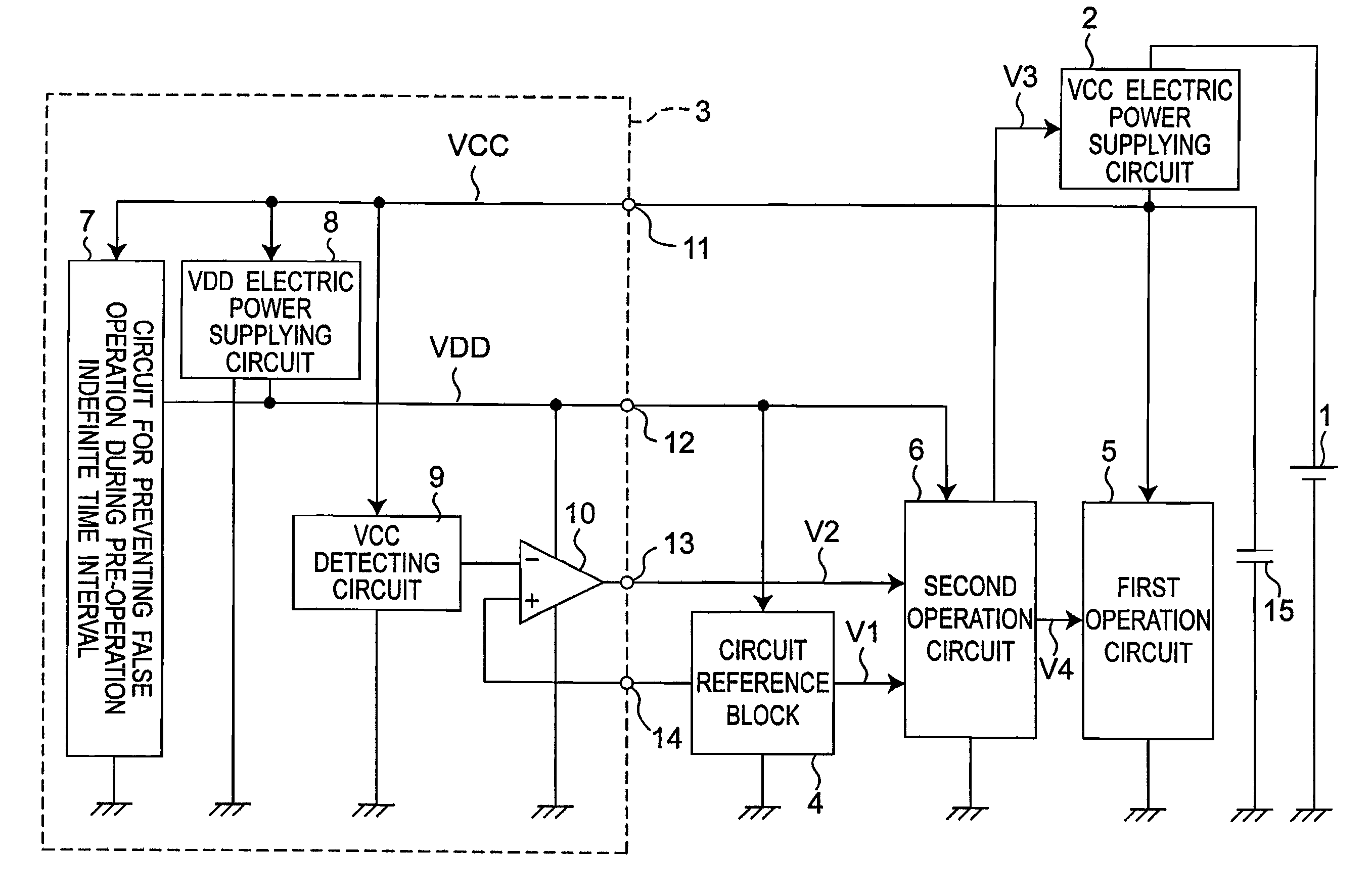
[0022]FIG. 1 is a circuit diagram showing a configuration of a semiconductor device provided with a reference supply voltage circuit 3 according to a preferred embodiment 1 of the present invention. The semiconductor device shown in FIG. 1 includes a power supply 1, a VCC electric power supplying circuit 2, a reference supply voltage circuit 3, a circuit reference block 4, a first operation circuit 5, a second operation circuit 6, and a capacitor 15. The reference supply voltage circuit 3 includes a circuit 7 for preventing any false operation during a pre-operation indefinite time interval, a VDD electric power supplying circuit 8, a VCC detecting circuit 9, a comparator 10, a VCC terminal 11, a VDD terminal 12, a V2 terminal 13, and a VBG terminal 14.

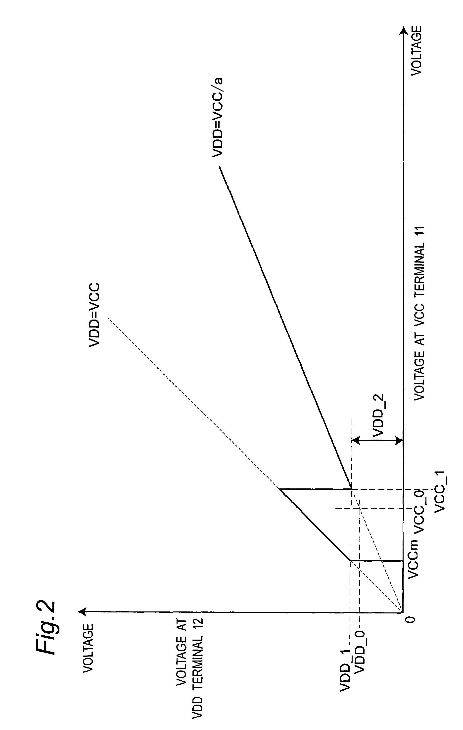
[0023]Referring to FIG. 1, an anode side of the power supply 1 is connected to the VCC electric power supplying circuit 2, and a cathode side thereof is connected to a ground potential. One side terminal of the c...

embodiment 2

Preferred Embodiment 2

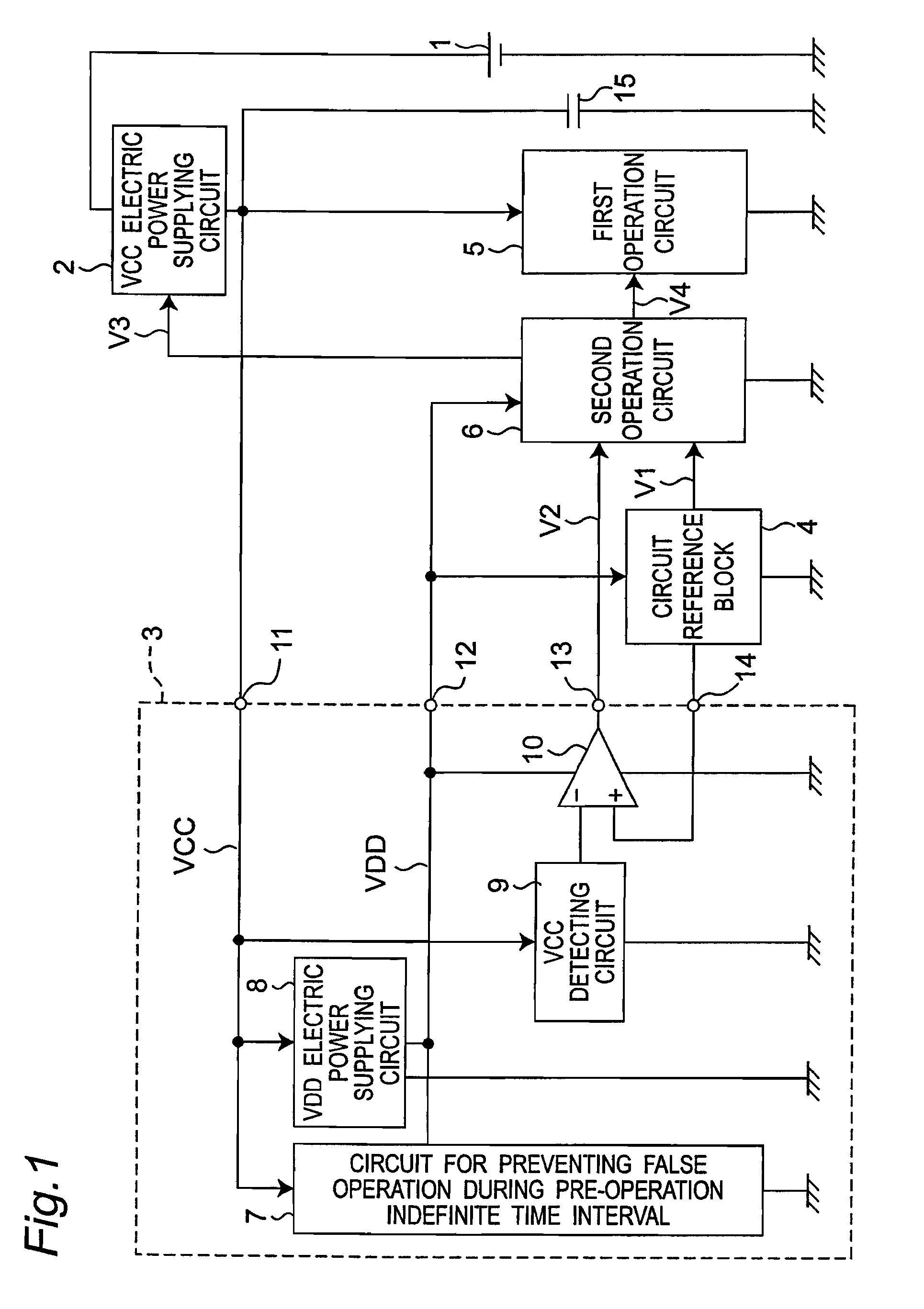
[0034]FIG. 3 is a circuit diagram showing a configuration of a semiconductor device provided with a reference supply voltage circuit 3A according to a preferred embodiment 2 of the present invention. The semiconductor device in the present preferred embodiment differs from the semiconductor device according to the preferred embodiment 1 shown in FIG. 1 in that the reference supply voltage circuit 3A is provided in place of the reference supply voltage circuit 3. The reference supply voltage circuit 3A includes a circuit 7A for preventing any false operation during a pre-operation indefinite time interval, a VDD electric power supplying circuit 8A, a VCC detecting circuit 9A, and a comparator 10A. In other respects, the configuration of the semiconductor device according to the present preferred embodiment is the same as that of the semiconductor device according to the preferred embodiment 1 shown in FIG. 1, and components labeled with the same reference numera...

embodiment 3

Preferred Embodiment 3

[0043]FIG. 5 is a circuit diagram showing a configuration of a semiconductor device provided with a reference supply voltage circuit 3B according to a preferred embodiment 3 of the present invention. The semiconductor device according to the present preferred embodiment differs from the semiconductor device according to the preferred embodiment 2 shown in FIG. 3 in that the reference supply voltage circuit 3B is provided in place of the reference supply voltage circuit 3A shown in FIG. 3. The reference supply voltage circuit 3B differs from the reference supply voltage circuit 3A according to the preferred embodiment 2 shown in FIG. 3 in that a circuit 7B for preventing any false operation during a pre-operation indefinite time interval is provided in place of the circuit 7A for preventing any false operation during the pre-operation indefinite time interval. The circuit 7B for preventing any false operation during the pre-operation indefinite time interval dif...


PUM


Abstract

A reference supply voltage circuit includes a detecting device for detecting a first reference voltage, a comparator, and a preventing circuit for preventing any false operation during pre-operation indefinite time interval. The comparator outputs a signal which controls an operation circuit whose supply voltage is a second reference voltage equal to or lower than the first reference voltage. The preventing circuit maintains the second reference voltage to a circuit reference potential when the first reference voltage is lower than a first predetermined voltage, sets the second reference voltage to a voltage equal to the first reference voltage when the first reference voltage is equal to or higher than the first predetermined voltage and lower than a second predetermined voltage, and sets the second reference voltage to a voltage proportional to the first reference voltage when the first reference voltage is equal to or higher than the second predetermined voltage.

Description

BACKGROUND OF THE INVENTION[0001]1. Field of the Invention[0002]The present invention relates to a reference supply voltage circuit, and particularly, relates to a reference supply voltage circuit which uses more than two reference supply voltages.[0003]2. Description of the Related Art[0004]There is disclosed in Japanese Patent Laid-Open Publication No. 2001-224169 a semiconductor device for a switching power supply of prior art which reduces electric power consumption to improve power supply efficiency by reducing switching loss during a light load by a simple configuration. A control circuit of the semiconductor device for the switching power supply has an error amplifier for generating an error voltage signal made from a difference between a supplemental supply voltage and a reference voltage, and an element current detecting comparator for comparing an element current detection signal detected by a current detecting circuit with the error voltage signal. Further, the control ci...

Claims


Application Information

Patent Timeline
Patent Type & Authority Patents(United States)
IPC IPC(8): G05F1/10
CPCG05F3/24
Inventor HACHIYA, YOSHIAKIARAKAWA, RYUTAROKUNIMATSU, TAKASHIFUKUI, MINORU
Owner PANASONIC CORP
Why Eureka
Try Eureka