Device including nonvolatile memory element

a non-volatile memory element and device technology, applied in the direction of solid-state devices, semiconductor devices, instruments, etc., can solve the problems of limiting the reduction of a proportion of the area occupied by the peripheral circuit, the inability to achieve stable reading operation, and the inability to increase the size of the memory cell array, etc., to achieve stable operation of the circuit, the leakage current of the non-selected memory cell can be extremely small, and the effect of stable operation

Active Publication Date: 2011-05-19
SEMICON ENERGY LAB CO LTD
View PDF99 Cites 24 Cited by
  • Summary
  • Abstract
  • Description
  • Claims
  • Application Information

AI Technical Summary

Benefits of technology

[0017]According to one embodiment of the present invention, a stable operation of a circuit can be realized when the circuit is formed using a nonvolatile memory element using an oxide semiconductor. The off-current of the nonvolatile memory element using an oxide semiconductor is extremely small; thus, the leakage current of a non-selected memory cell can be extremely small, leading to a stable operation, in particular, a stable reading operation. Moreover, since the leakage current of the bit line BL is extremely small, the number of memory cells which are connected to one bit line can be increased. Therefore, a device including a nonvolatile memory element which operates stably and is suitable for large capacity can be realized. Such a device including a nonvolatile memory element is particularly effective in the case where a transistor including an oxide semiconductor layer is provided in a pixel of a display device because the nonvolatile memory element and the pixel can be manufactured over one substrate.

Problems solved by technology

However, a nonvolatile memory element using a silicon-based semiconductor material has a problem in that a stable reading operation cannot be sufficiently obtained when the nonvolatile memory element has a larger capacity.
As a result, an increase in a memory cell array in size is difficult, and there has been a limitation on a reduction in a proportion of area occupied by a peripheral circuit.

Method used


Image

  • Device including nonvolatile memory element
  • Device including nonvolatile memory element
  • Device including nonvolatile memory element

Examples


embodiment 1

[0038]In this embodiment, a structure, a manufacturing method, and an operation principle of a device including a nonvolatile memory element according to one embodiment of the present invention will be described with reference to FIGS. 1A and 1B, FIGS. 2A to 2F, FIGS. 3A to 3D, and FIG. 4.

Plan Structure and Cross-Sectional Structure of Nonvolatile Memory Element

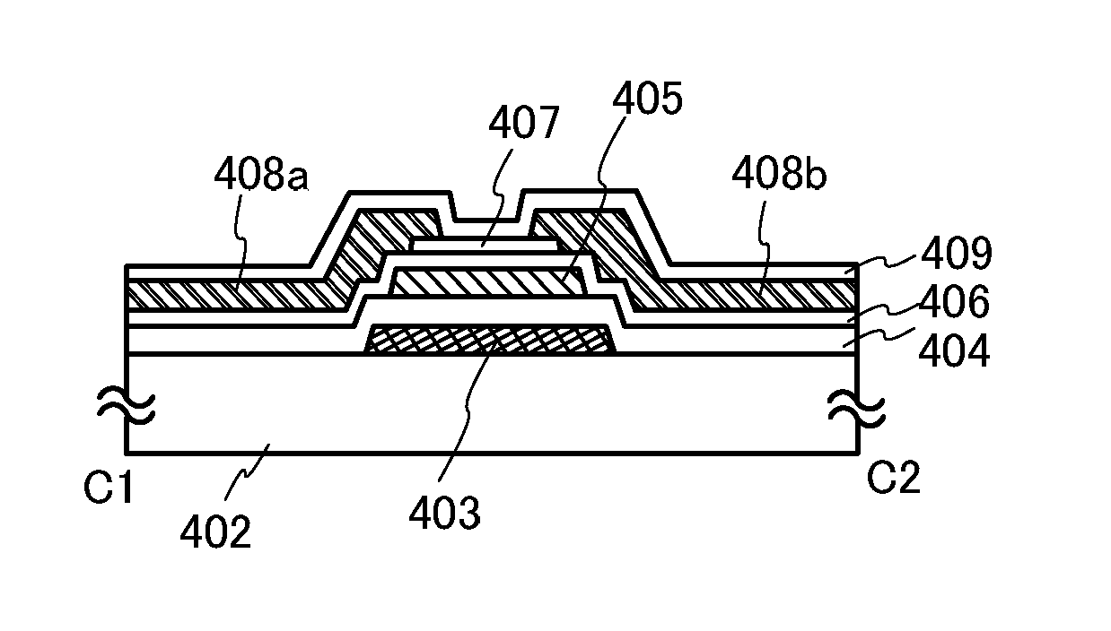
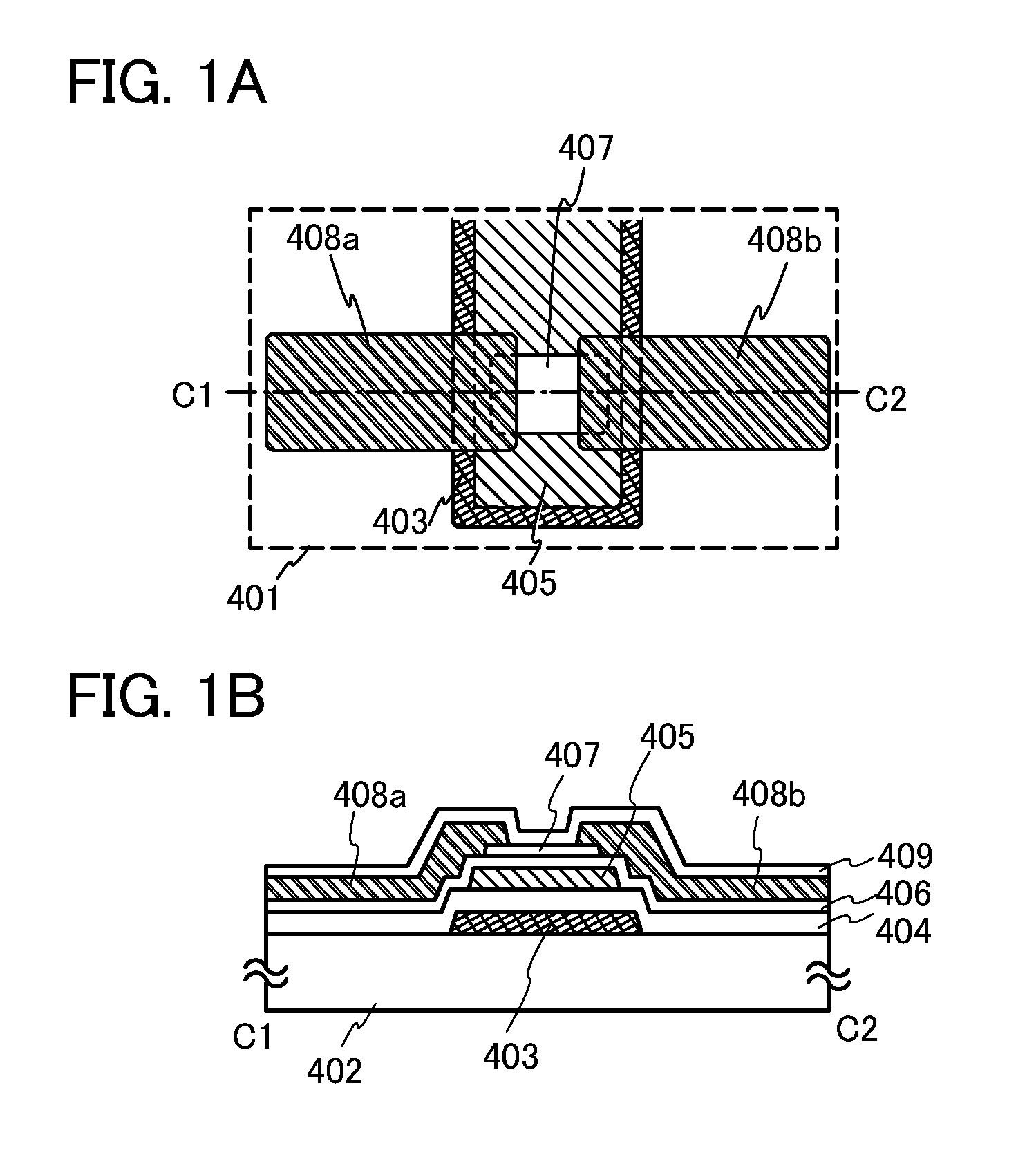
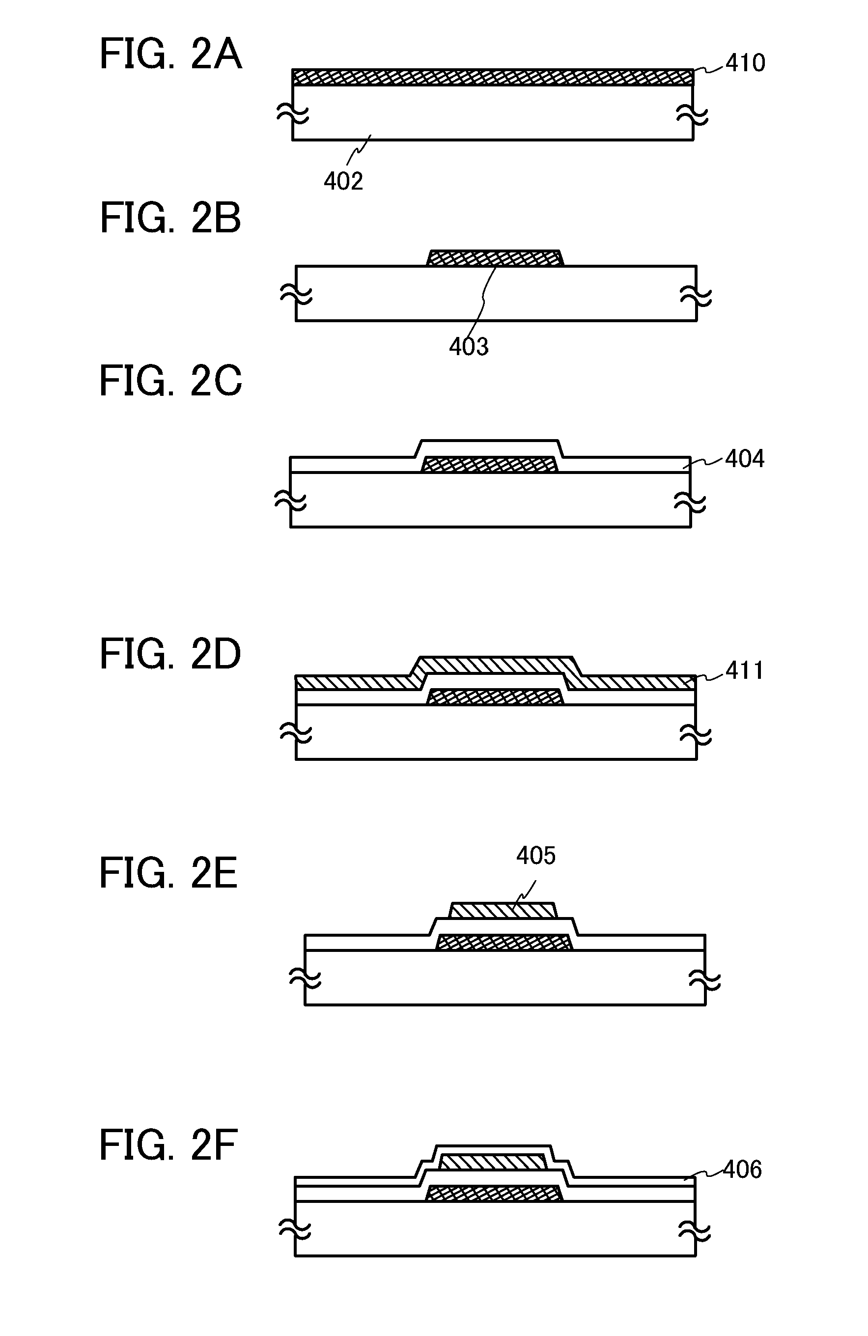
[0039]FIGS. 1A and 1B illustrate an example of a structure of a nonvolatile memory element. FIG. 1A is a plan view of the nonvolatile memory element and FIG. 1B is a cross-sectional view thereof. FIG. 1B corresponds to a cross-sectional view taken along line C1-C2 in FIG. 1A.

[0040]A nonvolatile memory element 401 includes a control gate 403 provided over a substrate 402, a first insulating film 404 which overlaps with the control gate 403, a charge accumulation layer 405 in contact with the first insulating film 404, a second insulating film 406 which overlaps with the charge accumulation layer 405, an oxide semiconductor lay...

embodiment 2

[0133]In this embodiment, a structure, which is different from the structure of FIGS. 1A and 1B, of a device including the nonvolatile memory element according to one embodiment of the present invention will be described with reference to FIGS. 5A and 5B. FIG. 5A is a plan view of the nonvolatile memory element and FIG. 5B is a cross-sectional view thereof. FIG. 5B corresponds to a cross-sectional view taken along line C1-C2 in FIG. 5A.

[0134]FIGS. 5A and 5B illustrate an example in which the pattern shape of the oxide semiconductor layer 407 is different from that of FIGS. 1A and 1B. The other structures are the same or substantially the same as the structures of FIGS. 1A and 1B; thus, description thereof is omitted.

[0135]In this embodiment, the oxide semiconductor layer 407 is provided so that the width of the oxide semiconductor layer 407 is larger than the width of the charge accumulation layer 405 in a channel length direction (a direction along line C1-C2). Thus, the widths of ...

embodiment 3

[0139]In this embodiment, a structure, which is different from the structure of FIGS. 1A and 1B, of a device including the nonvolatile memory element according to one embodiment of the present invention will be described with reference to FIGS. 6A to 6C. FIG. 6A is a plan view of the nonvolatile memory element and FIGS. 6B and 6C are each a cross-sectional view thereof. FIG. 6B corresponds to a cross-sectional view taken along line C1-C2 in FIG. 6A. FIG. 6C corresponds to a cross-sectional view taken along line D1-D2 in FIG. 6A.

[0140]FIGS. 6A to 6C illustrate an example in which the pattern shapes of the oxide semiconductor layer 407 and the source electrode 408a are different from those of FIGS. 1A and 1B. The other structures are the same or substantially the same as the structures of FIGS. 1A and 1B; thus, description thereof is omitted.

[0141]The oxide semiconductor layer 407 is provided so that the width of the oxide semiconductor layer 407 is larger than the width of the charge...


PUM


Abstract

A device including a novel nonvolatile memory element is provided. A device including a nonvolatile memory element in which an oxide semiconductor is used as a semiconductor material for a channel formation region. The nonvolatile memory element includes a control gate, a charge accumulation layer which overlaps with the control gate with a first insulating film provided therebetween, and an oxide semiconductor layer formed using an oxide semiconductor material, which overlaps with the charge accumulation layer with a second insulating film provided therebetween.

Description

TECHNICAL FIELD[0001]The present invention relates to a device including a nonvolatile memory element capable of electrical writing, reading, and erasing and a method for manufacturing the device. In particular, the present invention relates to a device including a nonvolatile memory element provided with a charge accumulation layer and a method for manufacturing the device.BACKGROUND ART[0002]The market has been expanded for nonvolatile memory elements in which data can be electrically rewritten and can be stored even after the power is turned off. Such nonvolatile memory elements have a structure similar to that of a metal oxide semiconductor field effect transistor (MOSFET), in which a charge accumulation layer capable of accumulating charges for a long time is provided between a channel formation region and a control gate. A silicon-based semiconductor material has been known as a semiconductor material for forming a channel formation region which can be applied to the nonvolati...

Claims


Application Information

Patent Timeline
Patent Type & Authority Applications(United States)
IPC IPC(8): H01L29/786
CPCG11C16/0466H01L21/28273H01L21/77H01L29/7881H01L27/12H01L27/1225H01L29/42324H01L27/11521H01L29/40114H10B41/30H10B41/10H01L29/66825
Inventor KATO, KIYOSHIIEDA, YOSHINORIKOYAMA, JUN
Owner SEMICON ENERGY LAB CO LTD
Why Eureka
Try Eureka