Compact processor element for a scalable digital logic verification and emulation system

a processor element and digital logic technology, applied in the field of electronic design of integrated circuits, can solve the problems that the embodiment of previous patents may not fully address the problems of ever larger, faster, more complex electronic system emulation and simulation, and achieve the effects of reducing the complexity of the emulation system, and maximizing the emulation system

Active Publication Date: 2009-03-24
EVE
View PDF5 Cites 6 Cited by
  • Summary
  • Abstract
  • Description
  • Claims
  • Application Information

AI Technical Summary

Benefits of technology

[0007]The present invention addresses the growth in size and complexity of electronic products which exceed the capacity or useful performance of conventional logic simulators. With arrays of the processors, a scalable system may contain and efficiently evaluate circuit signal values. Designers may determine in a timely manner if the design of a complex circuit does not provide the desired functionality or contains errors of timing or inadequate performance prior to the expense of fabricating the design in semiconductor manufacturing facilities. As a result electronic designers can bring a novel product to market sooner and at lower cost.

Problems solved by technology

Accordingly, the embodiments of previous patents may not fully addresses the issues of ever larger, faster, and more complex electronic system emulation and simulation.

Method used


Image

  • Compact processor element for a scalable digital logic verification and emulation system
  • Compact processor element for a scalable digital logic verification and emulation system
  • Compact processor element for a scalable digital logic verification and emulation system

Examples


Embodiment Construction

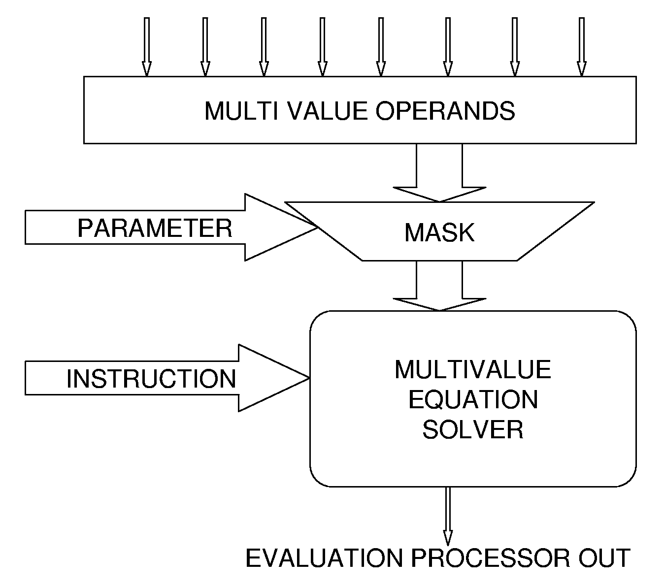
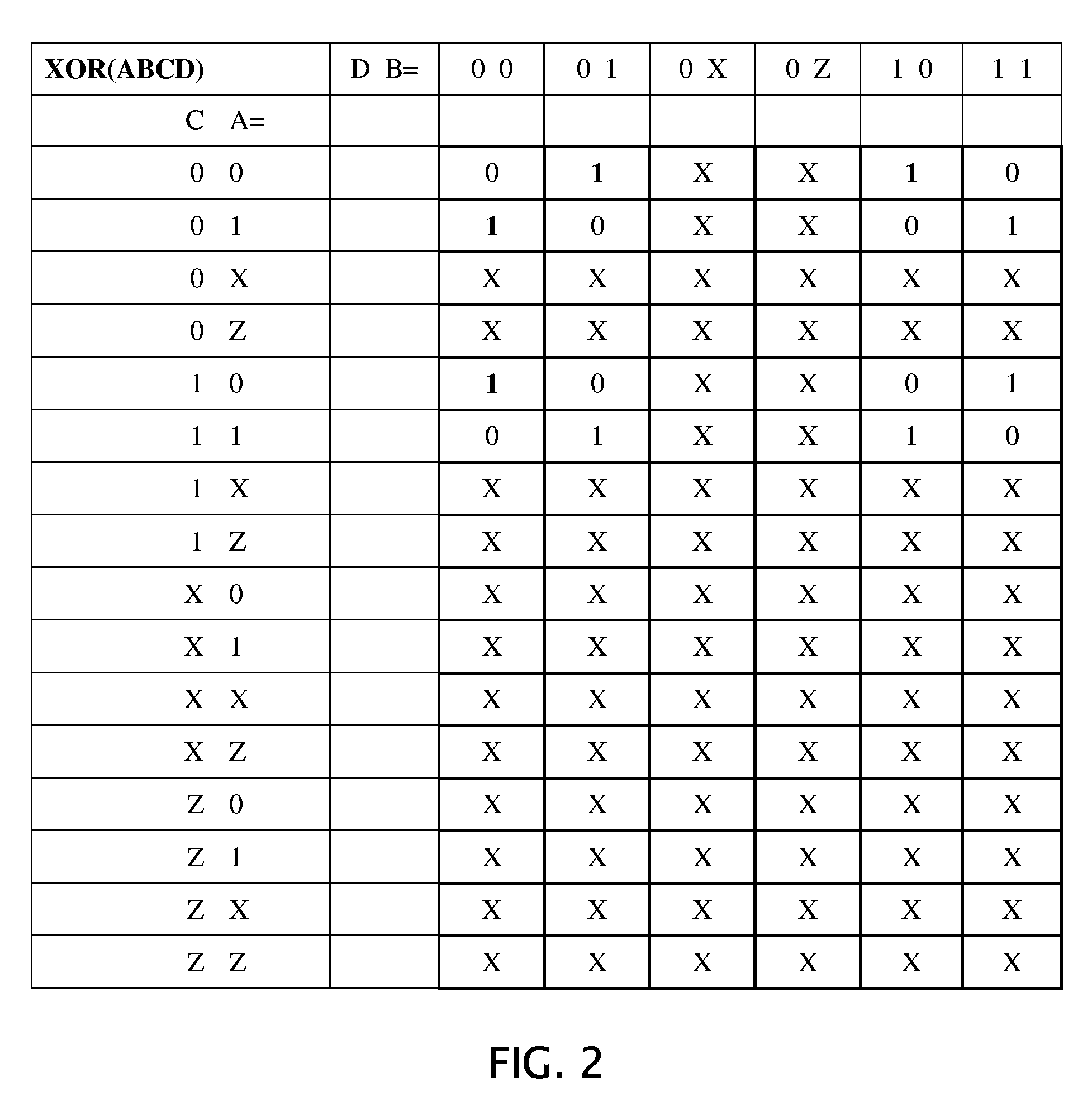
[0013]A processor is disclosed, for evaluating circuit signal values of an electronic design, comprising operand inputting ports for reading four or more operands, instruction input ports for reading one or more processor instructions, and encoding circuit drivers for encoding four or more circuit signal values onto a plurality of output bits.

[0014]The processor further has a number of inputs for reading one or more instruction parameters, the parameter comprising a specification of the operands to which the instruction applies. In an embodiment the processor can operate on up to 8 circuit signal values as inputs to a single instruction. Conventional simulators operate on the first two values and then operate on a third value with the result of the prior binary operation, as a result taking 7 cycles to accomplish the evaluation on 8 circuit signal values.

[0015]The processor further has decoding circuits for decoding four or more circuit signal values encoded in each operand, the val...


PUM


Abstract

A logic simulation acceleration processor optimized for multi-value logic level simulation of electronic systems described in hardware description languages.

Description

CROSS-REFERENCE TO RELATED APPLICATIONS[0001]The present application claims the benefit of priority under 35 USC .sctn. 119(e) from U.S. provisional patent application 60 / 595,057 filing date Jun. 2, 2005 first named inventor Ganesan, titled: “Massively parallel platform for accelerated verification of hardware and software.”FIELD OF THE INVENTION[0002]The present invention relates to the electronic design of integrated circuits, and more specifically to a method for the functional verification of a target integrated circuit design.RELATED ART[0003]Functional verification is one of the steps in the design of integrated circuits. Functional verification generally refers to determining whether a design representing an integrated circuit performs a function it is designed for. The inventors have previously disclosed functional verification systems (U.S. Pat. Nos. 6,691,287, 6,629,297, 6,629,296, 6,625,786, 6,480,988, 6,470,480, and 6,138,266) in which a target design is partitioned into...

Claims


Application Information

Patent Timeline
Patent Type & Authority Patents(United States)
IPC IPC(8): G06F17/50G06F15/80G06F7/38
CPCG06F17/5022G06F30/33
Inventor GANESAN, SUBBUBROUKHIS, LEONID ALEXANDERNARAYANASWAMY, RAMESHNIXON, IAN MICHAELSPENCER, THOMAS HANNI
Owner EVE
Why Eureka
Try Eureka