Nanotechnology-enabled optoelectronics

a technology of optoelectronics and nanotechnology, applied in the direction of laser optical resonator construction, laser details, semiconductor lasers, etc., can solve the problems of limiting the maximum available bandwidth, overloading the existing infrastructure, and unavoidable need to continue increasing the available bandwidth

Inactive Publication Date: 2009-04-07
NANOSYS INC
View PDF25 Cites 36 Cited by
  • Summary
  • Abstract
  • Description
  • Claims
  • Application Information

AI Technical Summary

Problems solved by technology

Thus, the migration of just this single industry onto the internet would completely overload the existing infrastructure.
As such, there is an unavoidable need to continue increasing available bandwidth within each fiber to meet capacity needs.
Both of these methods have problems, however, that will ultimately limit the maximum available bandwidth.
There are, of course, current practical limits to the available wavelength range defined by the transmission and dispersion of today's optical fibers; however, even these can efficiently transmit from 1200 nm to 1700 nm.
To date, however, the available wavelength range for telecommunications has been limited to a narrow spectral band around 1550 nm due to the narrow gain spectrum of erbium doped fiber amplifier (EDFA) (efficient gain from 1535 nm to 1570 nm).

Method used


Image

  • Nanotechnology-enabled optoelectronics
  • Nanotechnology-enabled optoelectronics
  • Nanotechnology-enabled optoelectronics

Examples


Embodiment Construction

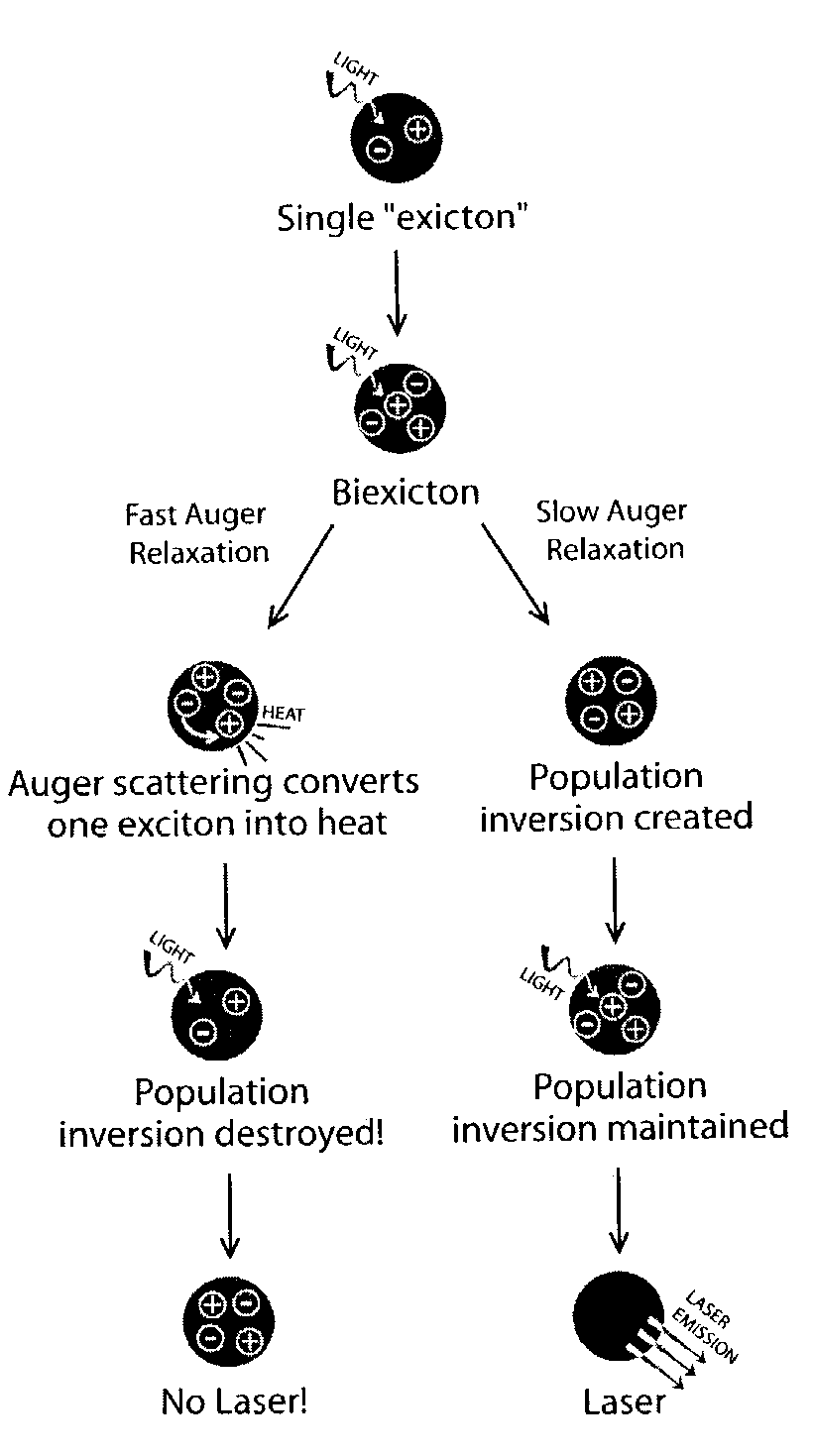
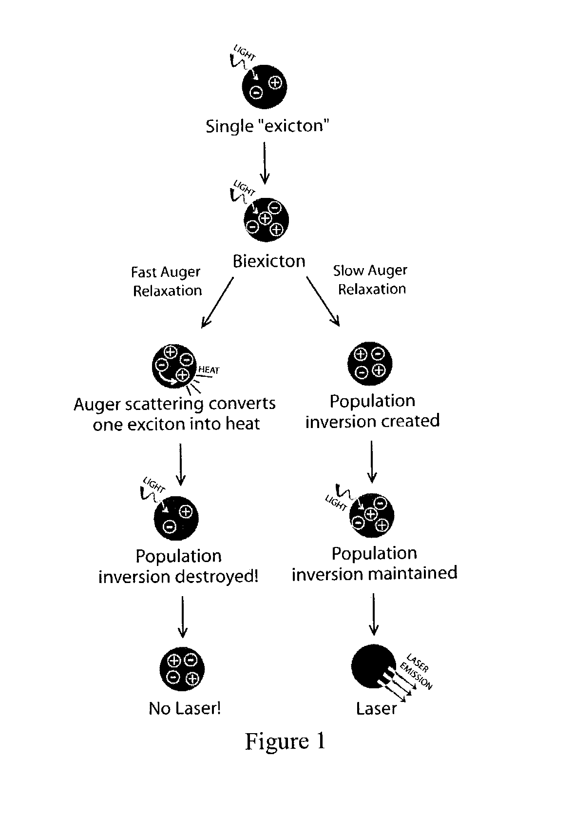
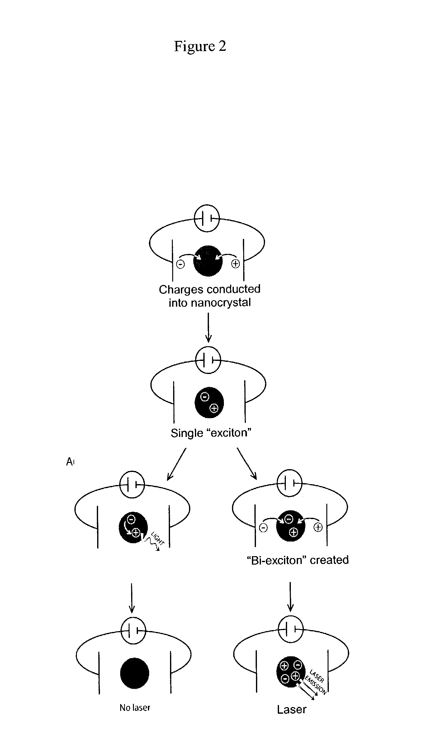
[0016]The present invention is generally directed to the use of nanomaterials, and particularly nanocrystals, e.g., nanodots, nanorods and three dimensional or branched nanocrystals in optoelectronic applications that are expected to result in a new generation of electrooptic devices where each microscopic step (absorption, emission, transport, charge injection, etc.) is independently and simultaneously optimized, while retaining low-cost high-volume processing.

[0017]Similar to today's semiconductor optical amplifiers (SOAs), the “nanocomposite optical amplifiers” (NOAs) described herein embody a broad-functioned technology with applications throughout the telecom industry. Unlike SOAs, however, NOAs can be fabricated and processed like a plastic. As a result, it is expected that these electrically addressable NOAs will have broad applications in, e.g., low-cost lasers, detectors, amplifiers, wavelength converters, switches and variable attenuators that function over a broad spectra...


PUM


Abstract

Nanomaterials for use in optoelectronic applications, and particularly nanocomposite optical amplifiers. nanocomposite optical amplifiers (NOAs), e.g., provided on integrated optical chips, for cost-effective broadband amplification across the entire clear-window of optical fiber. It is expected that such systems could provide a 15× increase in bandwidth over existing technology, while remaining compatible with all future advances in bit-rate and channel spacing.

Description

CROSS-REFERENCE TO RELATED APPLICATIONS[0001]This application claims priority to Provisional U.S. Patent Application No. 60 / 389,029, filed Jun. 13, 2002, the full disclosure of which is hereby incorporated herein by reference in its entirety for all purposes.BACKGROUND OF THE INVENTION[0002]The telecommunications industry has a defined set of performance and cost requirements, and an exponentially increasing demand for bandwidth. Even in today's market downturn, telecom network traffic still doubles approximately every year. Applications such as video on demand, telemedicine, interactive games and teleconferencing will increase the demands on the network infrastructure dramatically, outpacing the traditional technology. As an example, industry estimates suggest that there are about 100 million video rental transactions per week in the USA. Downloading this volume of information from the Internet would require a capacity of 40 terabits per second! In 2001, the Internet was believed t...

Claims


Application Information

Patent Timeline
Patent Type & Authority Patents(United States)
IPC IPC(8): H01S5/00H01S4/00
CPCB82Y20/00H01S5/341H01S3/169H01S5/10H01S5/3412H01S5/50Y10S977/815Y10S977/824Y10S977/819Y10S977/813Y10S977/818Y10S977/932Y10S977/834
Inventor EMPEDOCLES, STEPHEN
Owner NANOSYS INC
Why Eureka
Try Eureka