Eureka AIR delivers breakthrough ideas for toughest innovation challenges, trusted by R&D personnel around the world.

High resistivity silicon structure and a process for the preparation thereof

a silicon structure and high resistivity technology, applied in the direction of crystal growth process, after-treatment details, polycrystalline material growth, etc., can solve the problems of high manufacturing cost, lack of mechanical stability, material limitations, etc., and achieve high resistivity

Active Publication Date: 2009-04-21
GLOBALWAFERS CO LTD
View PDF24 Cites 13 Cited by
  • Summary
  • Abstract
  • Description
  • Claims
  • Application Information

AI Technical Summary

Problems solved by technology

Although FZ silicon is commercially available having resistivities of up to about 10 kohm-cm or more, this material has limitations.
For example, such material is expensive to manufacture, it lacks the mechanical stability needed for many applications, at least in part due to the low oxygen content therein, and it is of limited size.
Although CZ silicon addresses many of the limitations associated with FZ silicon, CZ silicon prepared by current techniques is also not without limitations.
Manufacturing CZ silicon in commercial environments to this level of purity, or beyond, is difficult and expensive.
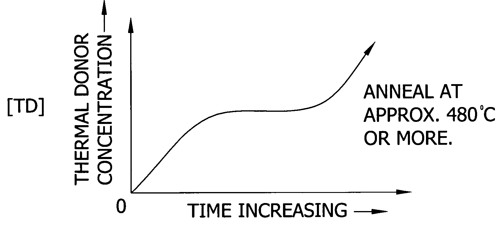
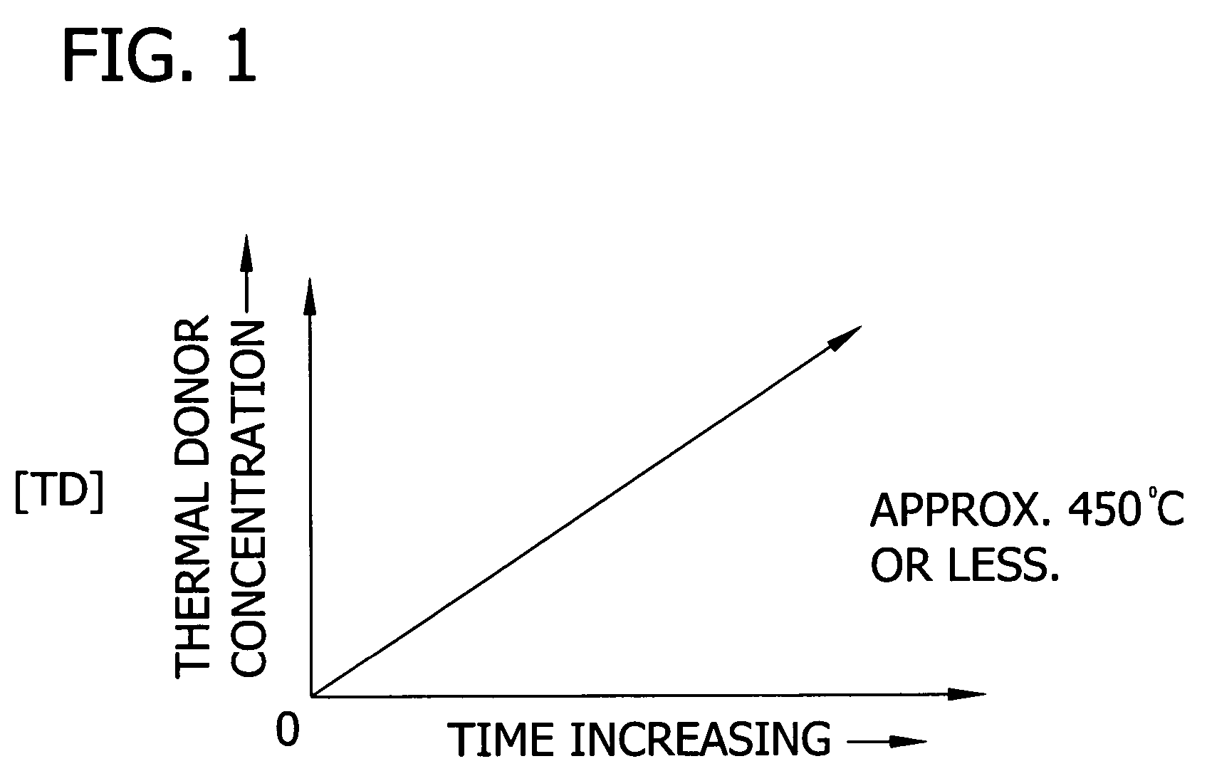
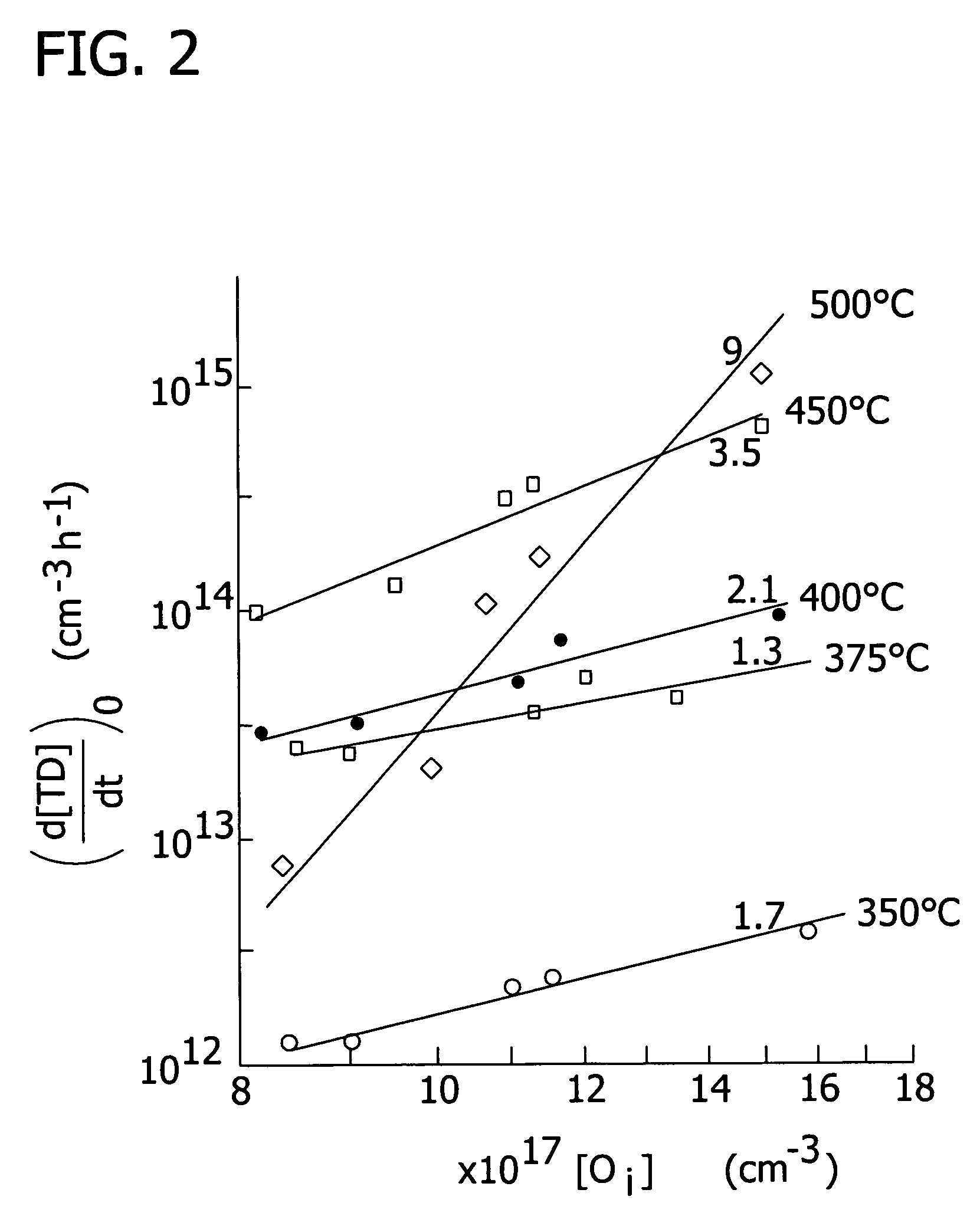
However, once such a low boron concentration is achieved, a second challenge exists, that being the presence of thermal donors.
However, this approach is costly and time consuming, involving long periods of time, typically tens of hours, at high temperatures.

Method used


Image

  • High resistivity silicon structure and a process for the preparation thereof
  • High resistivity silicon structure and a process for the preparation thereof
  • High resistivity silicon structure and a process for the preparation thereof

Examples


example 1

[0118]An example of the results that may be obtained using the techniques of the present invention, and as set forth in Equation (1a) herein, is found in FIG. 14. The resistivity data in FIG. 14 was obtained from Hall Effect determinations of carrier concentrations at different stages during the annealing of a wafer under conditions defined in this invention. In this example, a sample initially having a resistivity of about 300 ohm-cm (i.e., [B] equal to about 4e13 cm−3), and an oxygen concentration of about 6.5e17 cm−3, was used. The appropriate annealing temperature to achieve the high resistivity effect in a sample of this type was determined to be about 530° C. In this particular example, previously generated thermal donors were also present in the sample and the sample was actually n-type prior to the annealing (due to a prior 3 hour annealing at about 450° C.).

[0119]FIG. 14 shows the development of the resistivity, as deduced from the Hall Effect measurements, of this sample o...

example 2

[0121]Further to Example 1, above, and to demonstrate further the highly desirable “approximate” matching of conditions afforded by the present invention (and in accordance with Equation (1a) presented herein), samples similar to that used in Example 1 were annealed at temperatures near the calculated temperature of, in this instance, about 530° C. for this type of material. The results of the saturated resistivity following the anneal are shown in FIG. 15.

example 3

Comparative Example

[0122]This Example is to illustrate how the resistivity versus temperature curve, ρ(T), would look without a self-compensation effect.

[0123]In a simple “normal” case, when there is no reconstruction-based self-compensation, the resistivity is controlled essentially only by the achieved difference N=2Ntd(T,C)−NA. At N>0, the carrier (electron) concentration is n=N. At N<0, the carrier (hole) concentration is p=−N. More generally, at a very small difference N, the resistivity may approach the intrinsic value, and a more general expression for n and p may be used in this case (which is seldom to be met):

n=N / 2+[(N / 2)2+ni2]1 / 2,  (2)

p=−N / 2+[(N / 2)2+ni2]1 / 2,  (3)

where ni is the intrinsic electron concentration (close to about 1.3×1010 cm−3 at room temperature). The resistivity is ρ=1 / (eμnn+eμpp). The drift mobilities μn and μp are about 1,550 cm2 / sV and about 450 cm2 / sV, respectively (at room temperature).

[0124]The donor / acceptor difference, N, is convenient to write usin...


PUM


Abstract

The present invention generally relates to a high resistivity CZ silicon wafer, or a high resistivity silicon structure derived therefrom, and a process for the preparation thereof. In particular, the high resistivity silicon structure comprises a large diameter CZ silicon wafer as the substrate thereof, wherein the resistivity of the substrate wafer is decoupled from the concentration of acceptor atoms (e.g., boron) therein, the resistivity of the substrate being substantially greater than the resistivity as calculated based on the concentration of said acceptor atoms therein.

Description

CROSS-REFERENCE TO RELATED APPLICATION[0001]This application claims the benefit of U.S. Provisional Application 60 / 682,691, filed May 19, 2005, which is incorporated herein by reference.BACKGROUND OF THE INVENTION[0002]The present invention generally relates to a high resistivity CZ silicon structure, and a process for the preparation thereof. In particular, the high resistivity silicon structure comprises a large diameter CZ silicon wafer, or a substrate derived therefrom, wherein the resistivity of the wafer or substrate is decoupled from the concentration of acceptor atoms (e.g., boron) therein, the resistivity of the structure being substantially greater than the resistivity as calculated based on the concentration of said acceptor atoms therein. Such a wafer is particularly well-suited for use in, for example, high frequency (e.g., microwave or RF) applications.[0003]Traditionally, gallium arsenide (GaAs) wafers have been mostly used in high resistivity devices. Gallium arsenid...

Claims


Application Information

Patent Timeline
Patent Type & Authority Patents(United States)
IPC IPC(8): H01L21/00
CPCC30B29/06C30B33/00C30B33/02H01L21/3225H01L21/324
Inventor FALSTER, ROBERT J.VORONKOV, VLADIMIR V.VORONKOVA, GALINA I.BATUNINA, ANNA V.
Owner GLOBALWAFERS CO LTD
Why Eureka
Eureka Blog
Learn More