

High resistivity silicon wafer and method for fabricating the same
a high resistivity, silicon wafer technology, applied in the direction of silicon compounds, silicates, under a protective fluid, etc., can solve the problems of insufficient separation of n-wells, insufficient cmos characteristics, and insufficient p/n of wafers, so as to increase the depth of p/n, increase the release rate of oxygen, and high resistivity
- Summary
- Abstract
- Description
- Claims
- Application Information
AI Technical Summary
Benefits of technology
Problems solved by technology
Method used
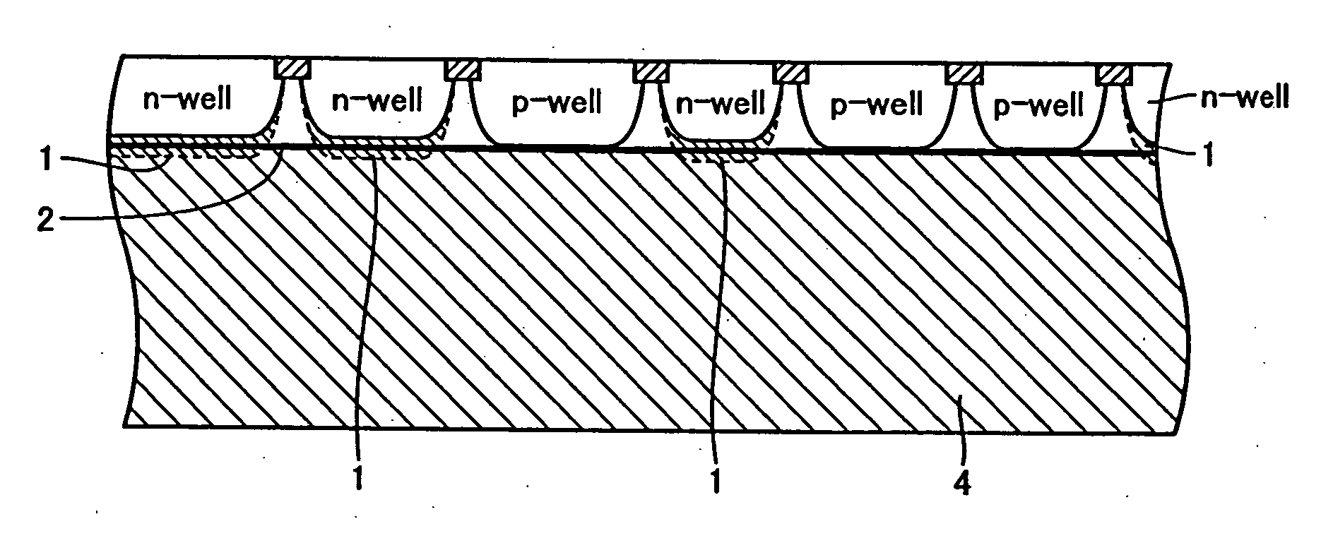
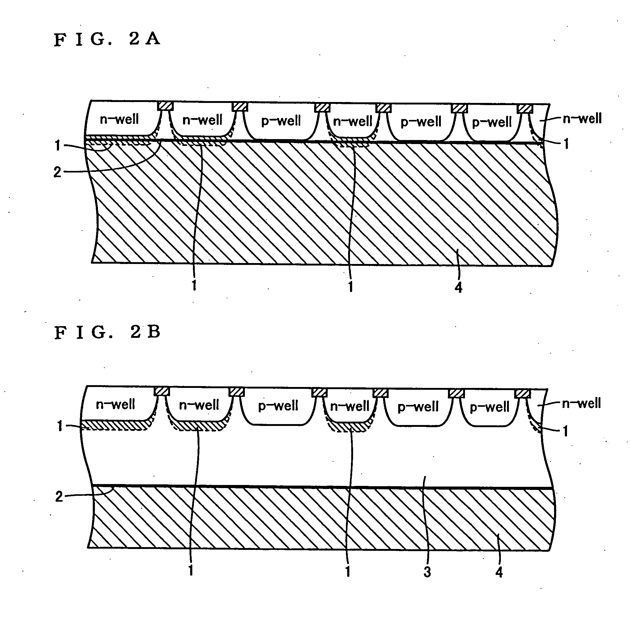
Image

Examples
examples
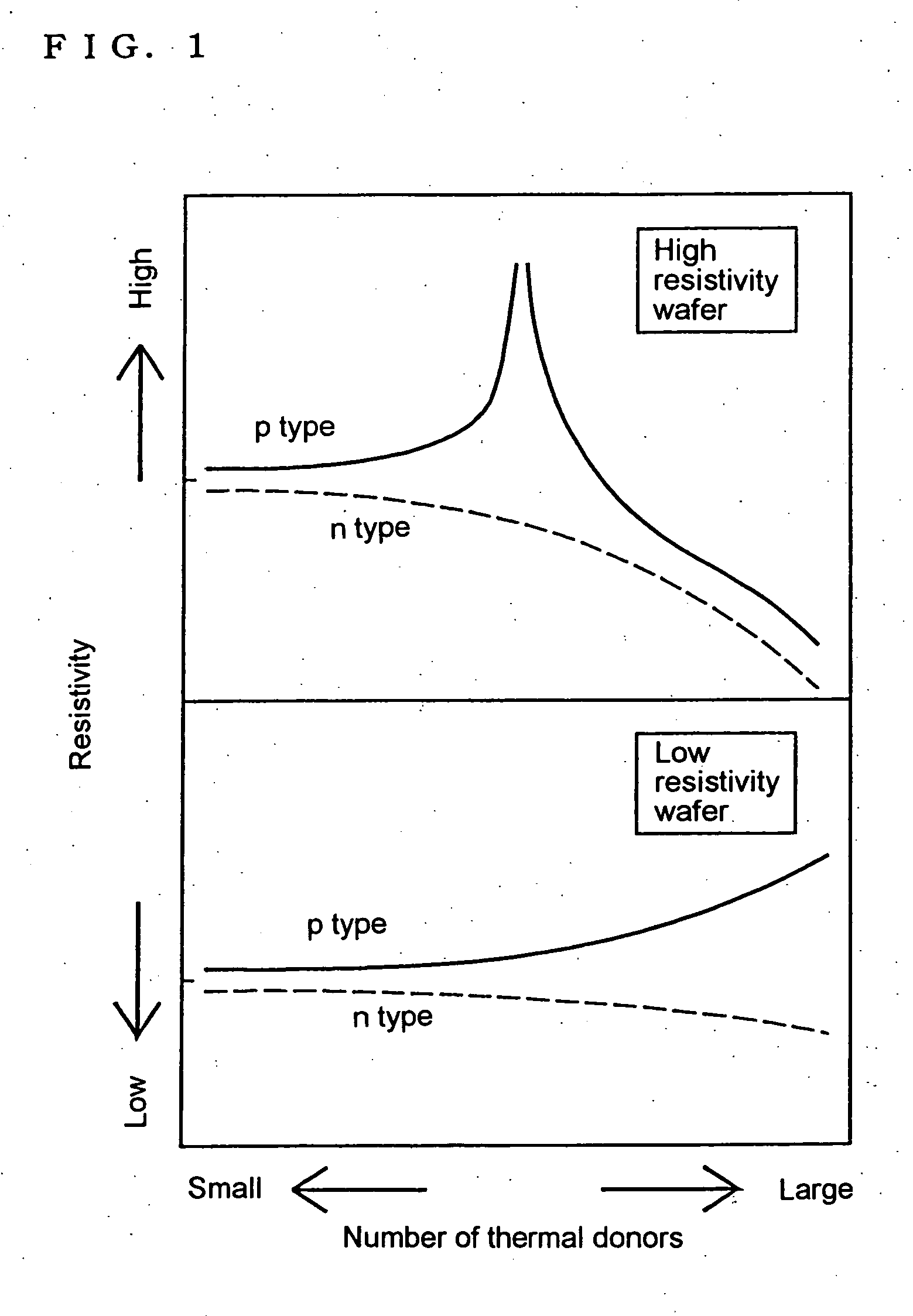
[0087] A p type wafer with an oxygen concentration of 13×1017 atoms / cm3 (ASTM F121-1979) and a carbon concentration of 2.5×10¹⁶ atoms / cm3 (ASTM F123-1981) and with a resistivity of 500 Ωcm, which is made by the CZ method, was prepared to make the following three kinds of wafers: [0088] A: to which no particular oxygen outward diffusion heat treatment has been applied; [0089] B: to which a heat treatment has been applied at 1200 degrees C. for 1 hour in hydrogen-gas atmosphere; and [0090] C: to which, after a 1 hour heat treatment at 1200 degrees C. in hydrogen-gas atmosphere, a further heat treatment has been applied at 700 degrees C. for 4 hours in nitrogen-gas with 3% of oxygen atmosphere, and subsequently at 1000 degrees C. for 16 hours.
[0091] After applying a heat treatment corresponding to a thermal history in the CMOS fabrication process shown in FIG. 4 to each of the wafers above, the resistivity distribution in the thickness direction was obtained by the measuring method fo...
PUM
| Property | Measurement | Unit |
|---|---|---|
| resistivity | aaaaa | aaaaa |
| resistivity | aaaaa | aaaaa |
| resistivity | aaaaa | aaaaa |
Abstract
Description
Claims
Application Information