

Polishing process for ultrahigh-resistivity silicon polished wafer
A silicon polishing sheet and resistivity technology, which is applied to surface polishing machine tools, grinding/polishing equipment, manufacturing tools, etc., can solve problems such as the difficulty in research and development of ultra-high resistivity silicon polishing sheets, and achieve simplified wax removal and cleaning procedures and Equipment, easy to clean, and the effect of improving flatness
- Summary
- Abstract
- Description
- Claims
- Application Information
AI Technical Summary
Problems solved by technology
Method used
Image

Examples
Embodiment
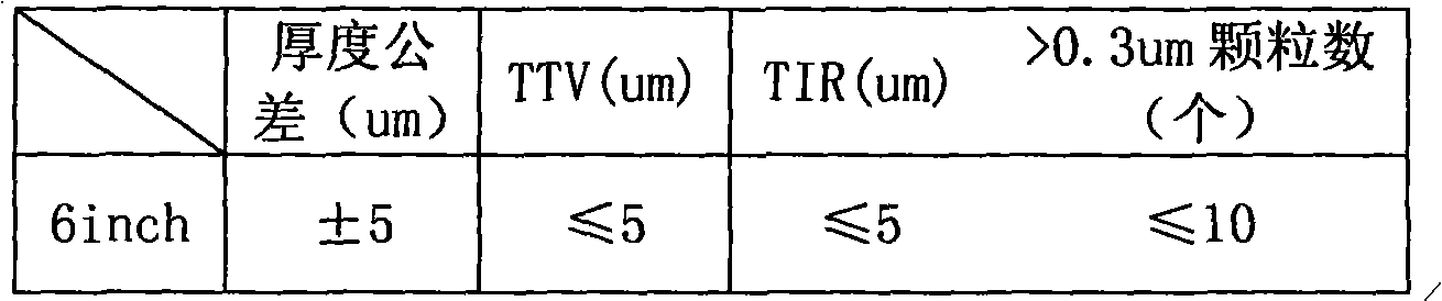
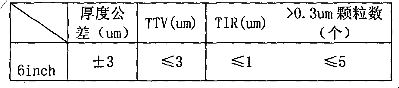
[0028] Embodiment: The wax-free polishing process of a 6-inch 500 μm thick ultra-high resistivity silicon wafer is as follows:
[0029] Experimental silicon wafer: 6-inch zone melting silicided wafer; crystal orientation: P; resistivity: 12000-20000Ω·cm; thickness: 520μm; quantity: 200 pieces.
[0030] Processing equipment: wax-free single-sided polishing system, rewinding machine, and unscrambling machine.
[0031] Auxiliary materials: rough polishing liquid, fine polishing liquid, deionized water.
[0032] Process parameters: The temperature of the polishing liquid is 35°C, and the temperature of the polishing machine plate is 45°C.
[0033] The pressure and time in the four steps of rough polishing are: ①, pressure: 2.55bar, polishing time: 3min; ②, pressure: 3.45bar, polishing time: 20min; ③, pressure: 1.25bar, polishing time: 15s;④ , Pressure: 1.25bar, Polishing time: 15s.
[0034] The pressure and time in the four steps of fine polishing are: ①, pressure: 1.55bar, pol...
PUM
| Property | Measurement | Unit |
|---|---|---|
| electrical resistivity | aaaaa | aaaaa |
| thickness | aaaaa | aaaaa |
Abstract
Description
Claims
Application Information