On-die termination circuit and method for semiconductor memory apparatus

a technology of semiconductor memory and on-die termination, which is applied in the direction of digital transmission, pulse technique, instruments, etc., can solve the problem of loss of signal proportion, and achieve the effect of preventing code adjustment errors

Active Publication Date: 2009-04-28
SK HYNIX INC
View PDF20 Cites 11 Cited by
  • Summary
  • Abstract
  • Description
  • Claims
  • Application Information

AI Technical Summary

Benefits of technology

[0014]Embodiments of the present invention have been made in order to solve the problems inherent in the related art, and embodiments of the present invention provide an on-die termination circuit and an on-die termination method for a semiconductor memory apparatus that can prevent code adjustment errors.

Problems solved by technology

In general, when a signal to be transmitted through a bus line having a predetermined impedance meets another bus line having a different impedance, a portion of the signal is lost.

Method used


Image

  • On-die termination circuit and method for semiconductor memory apparatus
  • On-die termination circuit and method for semiconductor memory apparatus
  • On-die termination circuit and method for semiconductor memory apparatus

Examples


first embodiment

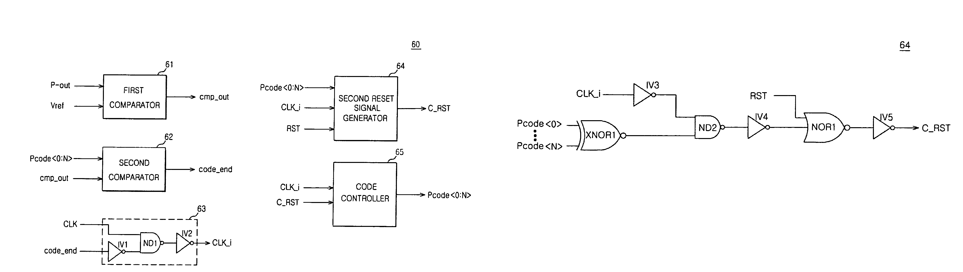
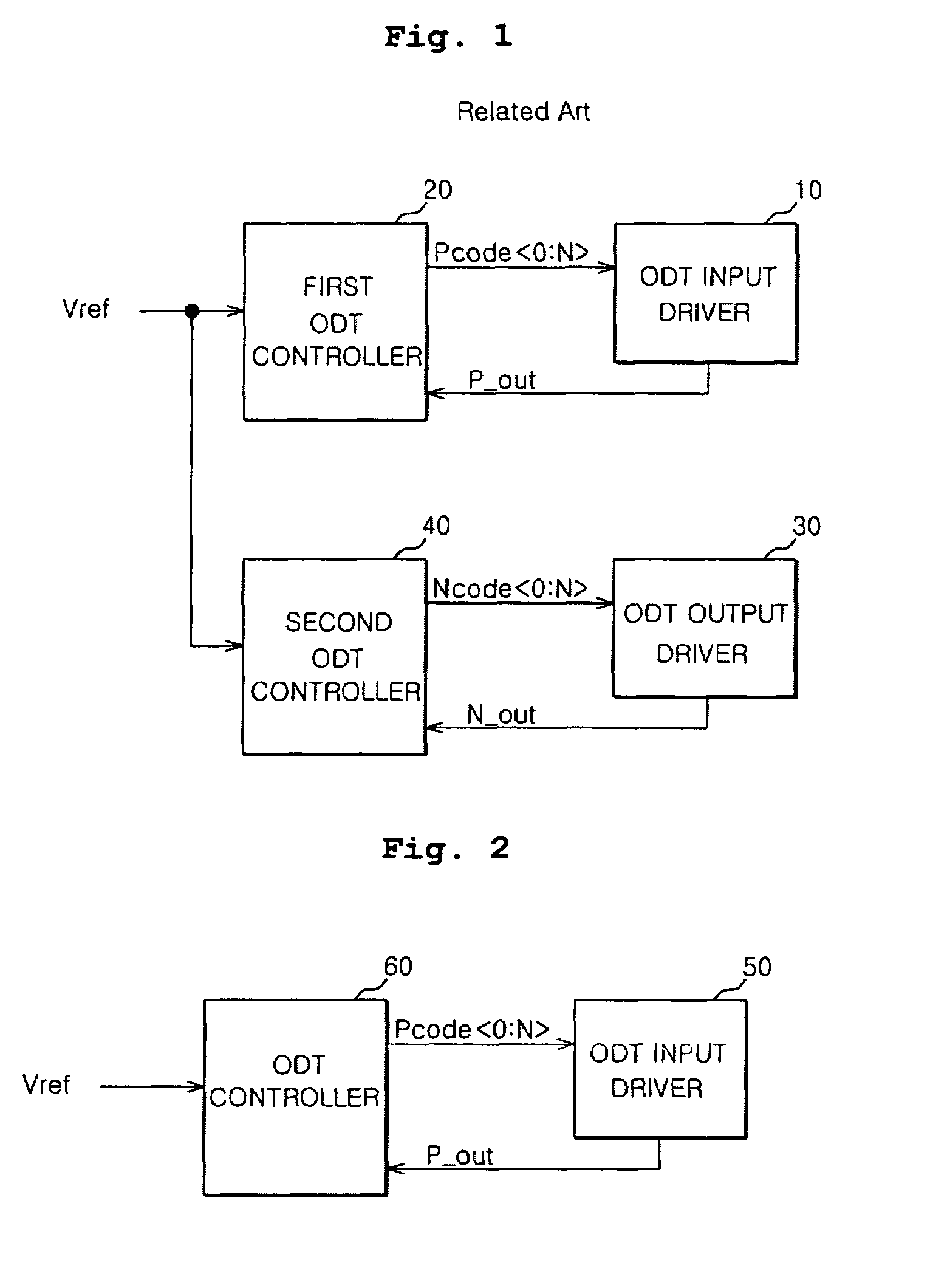
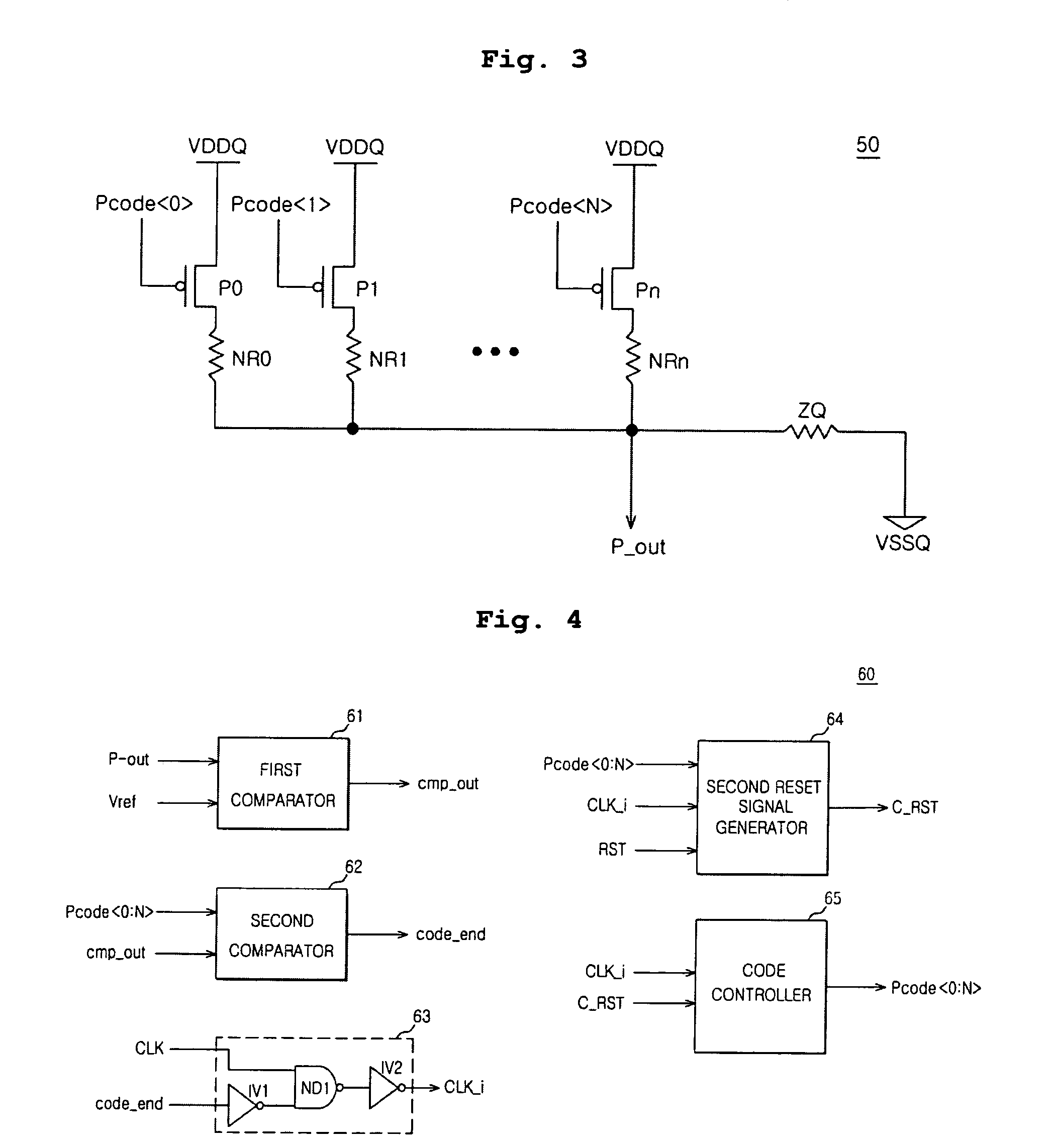
[0033]As shown in FIG. 2, an on-die termination circuit for a semiconductor memory apparatus according to an embodiment the present invention includes an ODT input driver 50 that receives a code Pcode having at least two bits, divides an input voltage on the basis of a resistance ratio according to the code Pcode, and outputs the divided voltage, and an ODT controller 60 that counts the code Pcode or resets the code Pcode to an initial value based on whether or not a line voltage P_out according to a resistance ratio of the ODT input driver 50 and a resistance ratio of an external resistor ZQ is consistent with a reference voltage Vref.

[0034]As shown in FIG. 3, the ODT input driver 50 includes a plurality of transistors P0 to Pn that are coupled to a power supply terminal VDDQ and are turned on according to the code Pcode, and a plurality of resistors NR0 to NRn that are respectively coupled between the plurality of transistors P0 to Pn and a ground terminal VSSQ.

[0035]As shown in F...

second embodiment

[0057]As shown in FIG. 7, an on-die termination circuit for a semiconductor memory apparatus according to a second embodiment of the present invention includes an ODT (On Die Termination) input driver 100 that divides an input voltage on the basis of a resistance ratio according to a first code Pcode having at least two bits and outputs a first line voltage P_out, a first ODT controller 200 that counts the first code Pcode or resets the first code Pcode to a first set value according to whether or not the first line voltage P_out and a reference voltage Vref are consistent with each other, an ODT output driver 300 that divides the input voltage on the basis of the resistance ratio of the first code Pcode and the resistance ratio of second code Ncode and outputs a second line voltage N_out, and a second ODT controller 400 that counts the second code Ncode or resets the second code Ncode to a second set value according to whether or not the second line voltage N_out and the reference ...


PUM


Abstract

An on-die termination circuit for semiconductor memory apparatus includes an ODT (On Die Termination) input driving unit that divides an input voltage on the basis of a resistance ratio according to a first code Pcode<0:N> having at least two bits and outputs a first line voltage, a first ODT control unit that counts the first code or resets the first code to a first set value according to whether or not the first line voltage and a reference voltage match with each other, an ODT output driving unit that divides an input voltage on the basis of the resistance ratio according to the first code and a resistance ratio according to a second code having at least two bits and outputs a second line voltage, and a second ODT control unit that counts the second code or resets the second code to a second set value according to whether or not the second line voltage and the reference voltage are consistent with each other.

Description

BACKGROUND OF THE INVENTION[0001]1. Technical Field[0002]The present invention relates to a semiconductor memory apparatus, and in particular, to an on-die termination circuit and an on-die termination method for a semiconductor memory apparatus.[0003]2. Related Art[0004]In general, when a signal to be transmitted through a bus line having a predetermined impedance meets another bus line having a different impedance, a portion of the signal is lost. Accordingly, an on-die termination (hereinafter, referred to as “ODT”) technique is used to match the impedance of the two bus lines with each other, to thereby reduce the signal loss.[0005]As shown in FIG. 1, an on-die termination circuit according to the related art includes an ODT input driver 10 that is modeled like a data input driver, which divides a power supply voltage VDDQ on the basis of a resistance ratio according to a first code Pcode<0:N>, and outputs a first line voltage P_out, a first ODT controller 20 that compares...

Claims


Application Information

Patent Timeline
Patent Type & Authority Patents(United States)
IPC IPC(8): H03K17/16H03K19/003
CPCG11C5/063G11C7/1051G11C7/1057G11C7/1078G11C7/1084H03K19/0005H04L25/0272H04L25/063H04L25/0298
Inventor PARK, JUNG-HOONYANG, SUN-SUK
Owner SK HYNIX INC
Why Eureka
Try Eureka