Method for manufacturing semiconductor device

a manufacturing method and semiconductor technology, applied in semiconductor devices, semiconductor/solid-state device details, electrical devices, etc., can solve the problems of not being able to provide interconnects or the like in a region, through electrodes, etc., to improve manufacturing stability, reduce parasitic capacitance, and enhance interconnect or element integration.

Inactive Publication Date: 2009-05-05
RENESAS ELECTRONICS CORP
View PDF11 Cites 26 Cited by
  • Summary
  • Abstract
  • Description
  • Claims
  • Application Information

AI Technical Summary

Benefits of technology

[0010]According to this method, it is possible to stably manufacture the semiconductor device with simple process that has a through electrode that is excellent in adhesion between the first plug and the second plug. Further, it is possible to manufacture the semiconductor device that is excellent in insulating property of the surface of the second plug with simple process.
[0027]As described above according to the present invention, there is provided the semiconductor device having the through electrode that is excellent in property as the electrode and manufacturing stability. Further, it is possible to make the interconnect of the semiconductor device to be high density.

Problems solved by technology

On the other hand, the through electrode described in the Japanese Laid-Open Patent Publication No. 2000-311982 has a configuration in which a large through electrode is penetrated through the semiconductor chip substrate, so that it is not possible to provide interconnect or the like on a region at which the through electrode is formed.

Method used


Image

  • Method for manufacturing semiconductor device
  • Method for manufacturing semiconductor device
  • Method for manufacturing semiconductor device

Examples


first embodiment

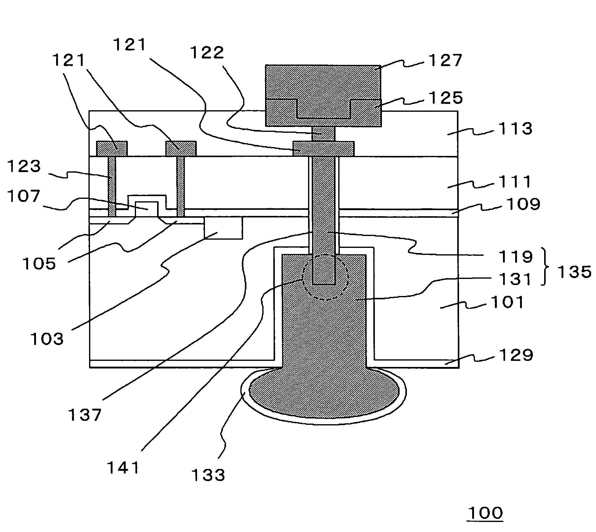
[0038]FIG. 1 is a sectional view schematically showing a configuration of a semiconductor device according to the present embodiment. The semiconductor device 100 shown in FIG. 1 has a multilayered structure formed by a silicon substrate 101, an etching stopper film 109, a lowermost-layer insulating film 111 and a first interconnect layer insulating film 113, and is provided with a through electrode 135 penetrating the silicon substrate 101, the etching stopper film 109 and the lowermost-layer insulating film 111.

[0039]A MOS transistor composed of a diffusion layer 105, a gate electrode 107 and the like and an isolation film 103 are formed on a main face of the silicon substrate 101. The lowermost-layer insulating film 111 is formed so as to embed the MOS transistor and the isolation film 103. The etching stopper film 109 is provided in the lowermost-layer insulating film 111 in contact with an upper face of the silicon substrate 101 and the gate electrode 107. Further, also a conne...

second embodiment

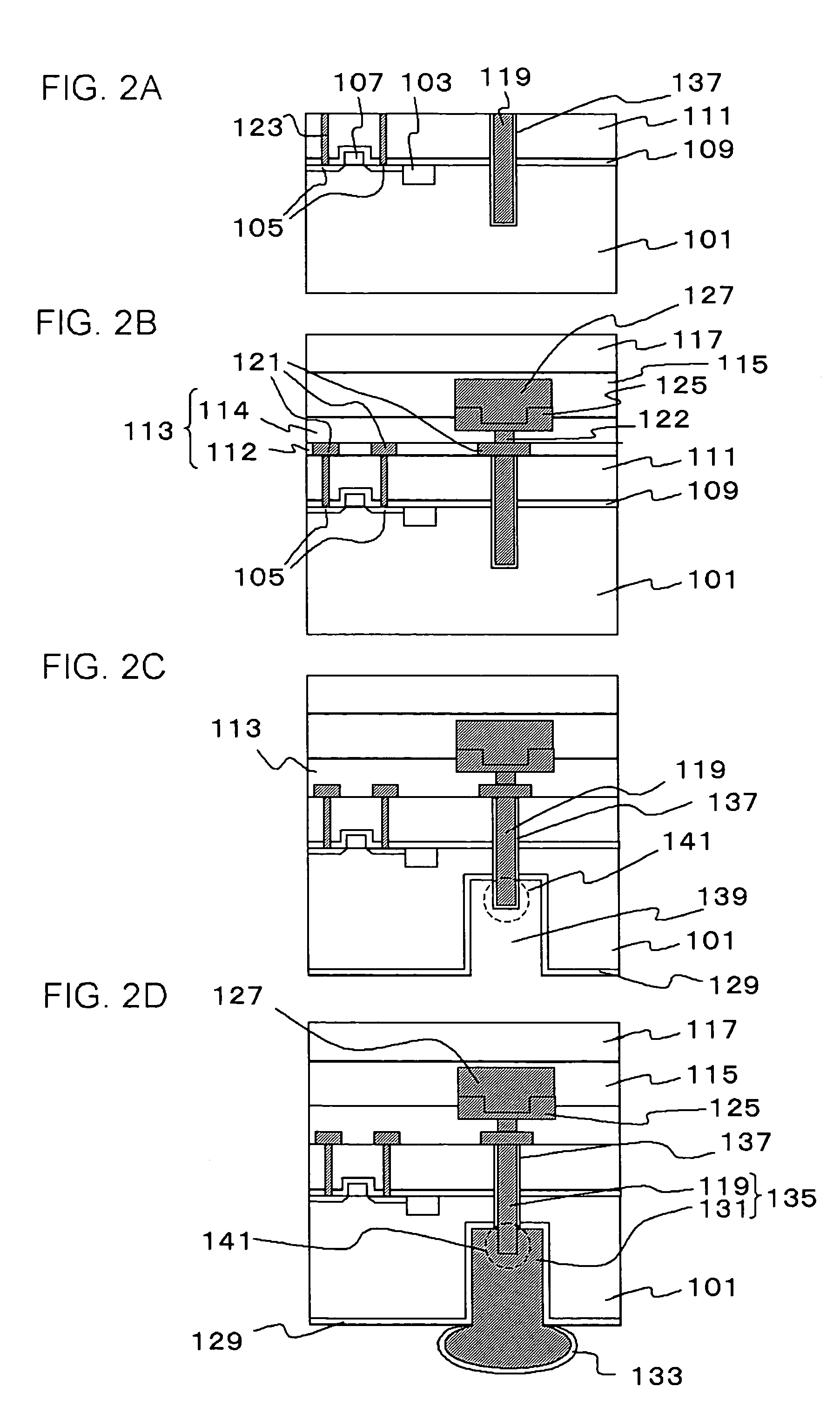
[0090]It is also possible to manufacture the semiconductor device 100 described in the first embodiment in such a way as the following process. Hereinafter, there will be described the embodiment about the point different from the first embodiment while referring to FIG. 2A to FIG. 2D.

[0091]First, like the first embodiment, process until providing the electrodeposited insulating film 129 on the rear surface of the silicon substrate 101 is performed (FIG. 2C). Next, in the same process as the first embodiment, the etching back of the SiN film 137 in the projecting portion 141 is performed.

[0092]Then, a metal seed layer is formed on the entire rear surface of the silicon substrate 101 on which the electrodeposited insulating film 129 is provided. The metal composing the seed layer may be, for instance, Ni, Ni / Cu, or TiN / Ti / Cu or the like. When using a plurality of metals in the seed layer, these are indicated in such a way as being “lower layer / upper layer” or “lower layer / intermediat...

third embodiment

[0096]It is also possible to manufacture the semiconductor device 100 described in the first embodiment in such a way as the following process. Hereinafter, there will be described the present embodiment about the point different from the first embodiment or the second embodiment while referring to FIG. 2A to FIG. 2D.

[0097]First, like the first embodiment and the second embodiment, the process described above using FIG. 2A and FIG. 2B is performed. The adhesive layer 115 is formed on the upper face of the silicon substrate 101, followed by adhering it to the supporting component 117 (FIG. 2B). After that, process until grinding the rear surface of the silicon substrate 101, and formation of the opening 139 is performed.

[0098]Next, the seed layer is provided on the rear surface of the silicon substrate 101, before performing process providing the electrodeposited insulating film 129 on the rear surface of the silicon substrate 101 (FIG. 2C). The material of the seed layer is material...


PUM


Abstract

A semiconductor device has through electrodes with property as an electrode and excellent in manufacturing stability. The through electrode composed of a conductive small diameter plug and a conductive large diameter plug is provided on the semiconductor device. A cross sectional area of the small diameter plug is made larger than a cross sectional area of a connection plug and its diameter each, and the cross sectional area of the small diameter plug is made smaller than a cross sectional area of the large diameter plug and its diameter each. Further, a projecting portion where the small diameter plug is projected from a silicon substrate is put into an upper face of the large diameter plug. Further, an upper face of the small diameter plug is connected to a first interconnect.

Description

[0001]This application is based on Japanese patent application NO. 2004-108442, the content of which is incorporated hereinto by reference.BACKGROUND OF THE INVENTION[0002]1. Field of the Invention[0003]The present invention relates to a method for manufacturing a semiconductor device.[0004]2. Related Art[0005]In recent years a semiconductor device necessitates to be lightweight, thin, and short sized, and a high performance. In the semiconductor device such as a multi-chip package or the like, realizing high density interconnect, miniaturization of a logic chip and capacity increase of a memory is aggressively promoted.[0006]As one corresponding means coping with such proposals, it is tried that realizing high density interconnect or the like is achieved upon providing a through electrode in a semiconductor substrate. For instance, the Japanese Laid-Open Patent Publication No. 2000-311982 discloses a conventional through electrode. The Japanese Laid-Open Patent Publication No. 2000...

Claims


Application Information

Patent Timeline
Patent Type & Authority Patents(United States)
IPC IPC(8): H01L21/44H01L23/52H01L21/3205H01L21/768H01L23/48H01L23/485
CPCH01L21/76898H01L23/481H01L24/13H01L24/10H01L2924/13091H01L2924/014H01L2224/13099H01L2224/16H01L2924/01013H01L2924/01022H01L2924/01029H01L2924/01074H01L2924/01078H01L2924/01079H01L2924/04953H01L2924/10329H01L2924/30105H01L2924/01005H01L2924/01006H01L2924/01033H01L2924/00H01L24/05H01L24/11H01L2224/0401H01L2224/05025H01L2224/05085H01L2224/05147H01L2224/05557H01L2224/05572H01L2224/05624H01L2224/05647H01L2224/05655H01L2224/13H01L2224/13009H01L2224/13025H01L2224/131H01L2224/13144H01L2224/13155H01L2224/14181H01L2924/00014
Inventor SOEJIMA, KOJIKAWANO, MASAYA
Owner RENESAS ELECTRONICS CORP
Why Eureka
Try Eureka