Optoelectronic system for sensing an electromagnetic field at total solid angle by having at least one optical modulator to change the intensity of an optical wave
an optoelectronic system and electromagnetic field technology, applied in the direction of optical radiation measurement, distance measurement, instruments, etc., can solve the problems reduce sensing accuracy, and achieve the effect of reducing sensing accuracy and easy cause of signal distortion in sensing
- Summary
- Abstract
- Description
- Claims
- Application Information
AI Technical Summary
Benefits of technology
Problems solved by technology
Method used
Image

Examples
first embodiment
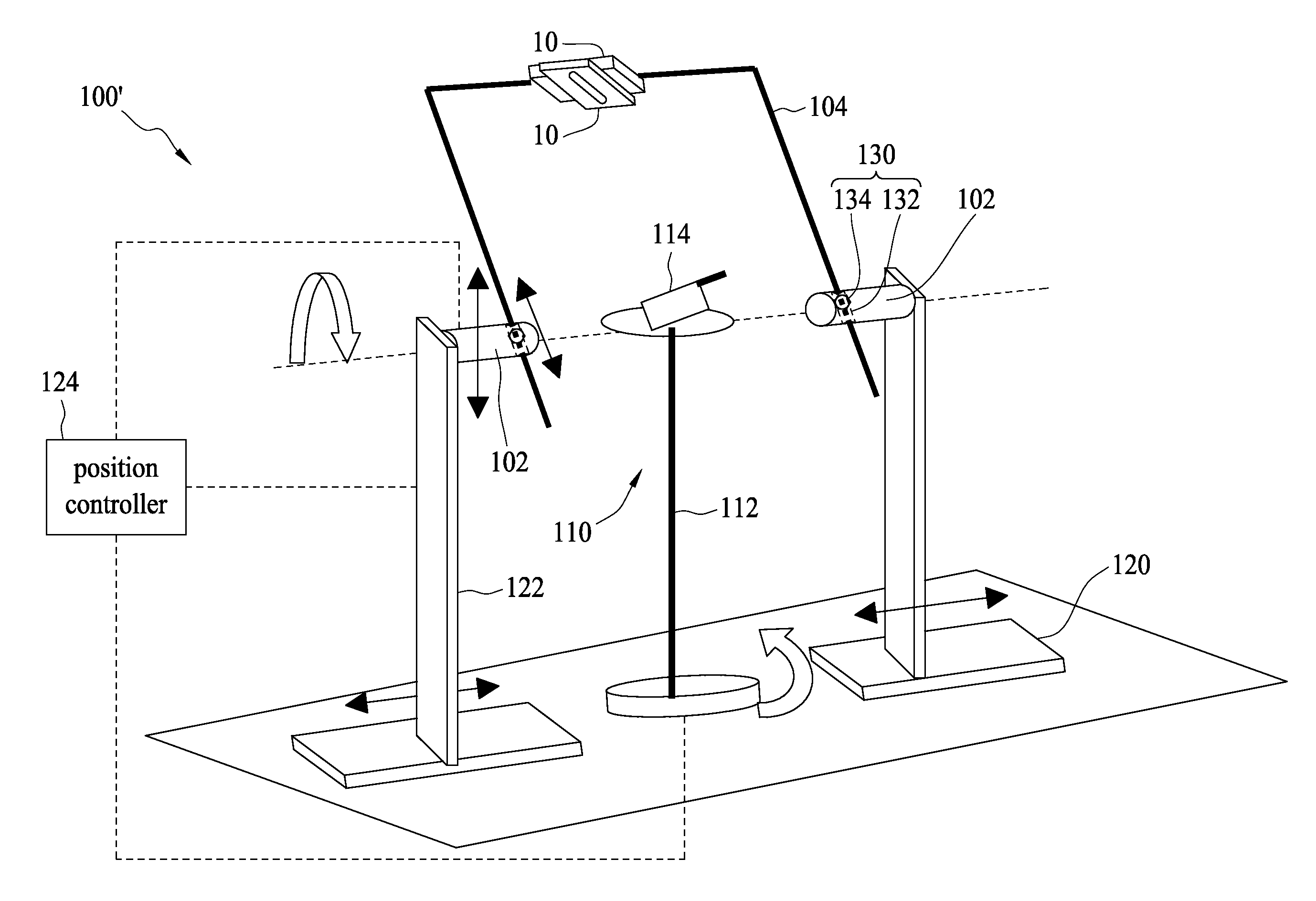
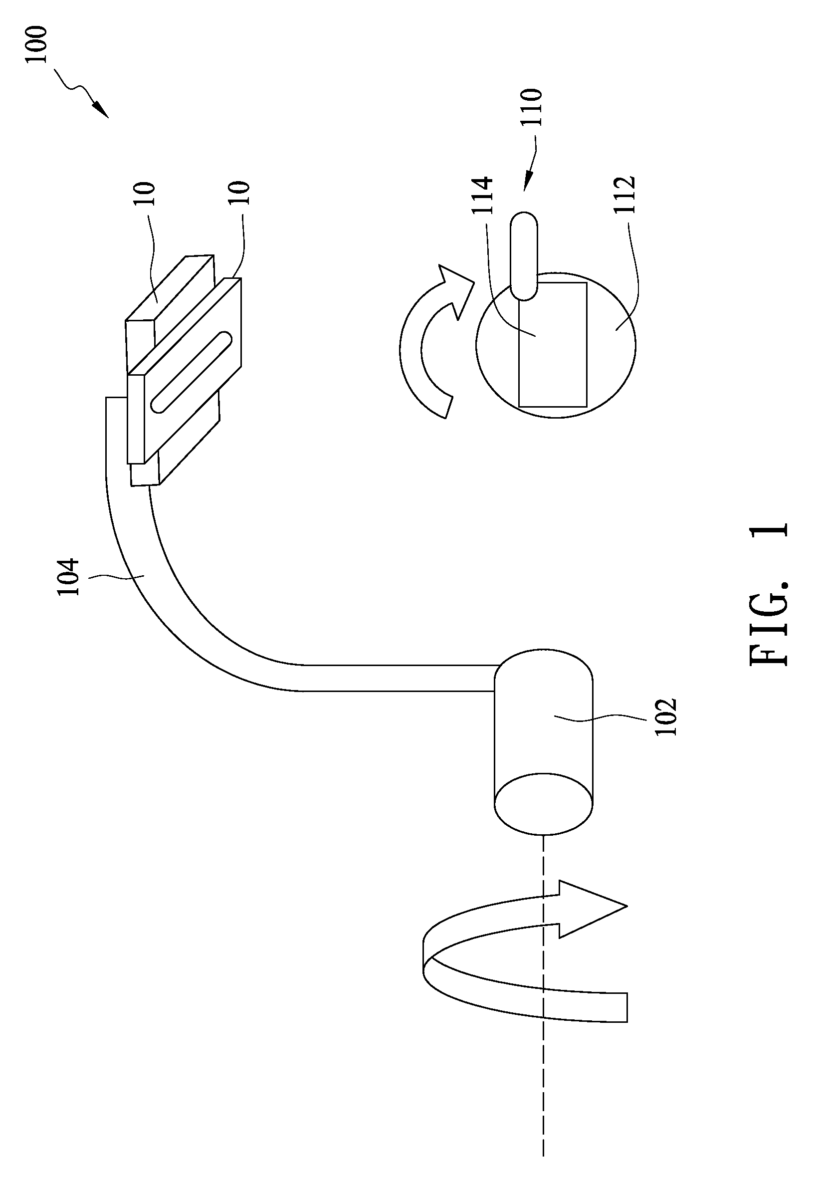
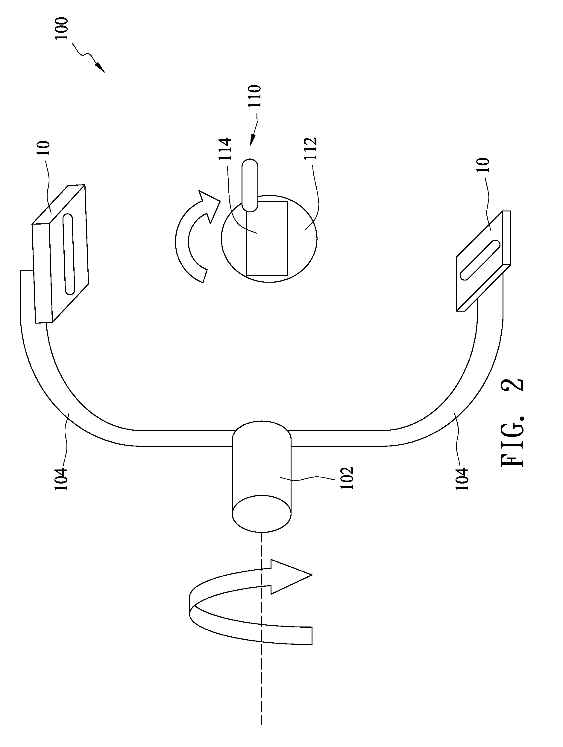
[0017]FIG. 1 illustrates an optoelectronic system 100 for sensing an electromagnetic field at total solid angle according to the present invention. The optoelectronic system 100 includes a first rotating shaft 102, at least one cantilever 104 disposed on the first rotating shaft 102, a rotating stand 110 configured to load an emission source 114 under test and at least one optoelectronic module 10 disposed on a free end of the cantilever 104 and configured to sense an electromagnetic signal emitted from the emission source 114 (for example, a handset) under test. The rotating stand 110 has a second rotating shaft 112 perpendicular to the first rotating shaft 102. Preferably, the optoelectronic system 100 includes two optoelectronic sensing modules 10 positioned in an orthogonal manner. Further, the optoelectronic system 100 includes two cantilevers 104 spaced 180° apart and two optoelectronic modules 10 positioned on the two free ends of the two cantilevers in an orthogonal manner, ...
second embodiment
[0020]FIG. 5 illustrates an optoelectronic module for sensing an electromagnetic field 10′ according to the present invention. The optoelectronic module 10′ includes an optical modulator 20′ and an external antenna 70. Compared with the optoelectronic module 10 in FIG. 3 which uses a built-in antenna 22, the optoelectronic module 10′ in FIG. 5 employs an external dipole antenna (i.e., an external antenna 70). In addition to disposing electrodes 52A, 52B on the outer sides of the optical modulation waveguides 18A, 18B respectively and disposing an electrode 54 between the electrodes 52A, 52B, the structure of the optical modulator 20′ is substantially similar to the optoelectronic module 10 in FIG. 3, wherein the phase of a laser beam propagating therethrough can be changed based on an applied electric field.
[0021]The external antenna 70 senses the electric field and magnetic field of the emission source 112 under test, and applies a potential difference to the electrodes 52A, 52B, 5...
third embodiment
[0023]FIG. 7 illustrates an optoelectronic module 10″ for sensing an electromagnetic field according to the present invention. Compared with the optoelectronic module 10 in FIG. 3, the optoelectronic module 10″ in FIG. 7 includes an optical circulator 60 and an optical modulator 20″. In particular, the optical circulator 60 includes a first port 61, a second port 62, and a third port 63. The laser beam emitted from the laser source 34 is input into the optical circulator 60 via the first port 61 and output from the second port 62. The optical modulator 20″ is connected to the second port 62, and the optical detector 30 is connected to the third port 63. The optical modulator 20″ includes a substrate 12, a mirror 13 disposed on a side surface of the substrate 12, an optical input / output waveguide 15 disposed in the substrate 12, two optical modulation waveguides 18A, 18B disposed in the substrate 12 and an antenna 22 disposed on the surface of the substrate 12. One end of the optical...
PUM
 Abstract
Description
Claims
Application Information
 - R&D Engineer
- R&D Manager
- IP Professional
- Industry Leading Data Capabilities
- Powerful AI technology
- Patent DNA Extraction
Browse by: Latest US Patents, China's latest patents, Technical Efficacy Thesaurus, Application Domain, Technology Topic.
© 2024 PatSnap. All rights reserved.Legal|Privacy policy|Modern Slavery Act Transparency Statement|Sitemap