

Method for compacting the erased threshold voltage distribution of flash memory devices during writing operations
a flash memory device and threshold voltage technology, applied in the field of electronic devices, can solve the problems of wide erased distribution, unfavorable logic value storage in the cell, and particularly acute problems,
- Summary
- Abstract
- Description
- Claims
- Application Information
AI Technical Summary
Benefits of technology
Problems solved by technology
Method used
Image

Examples
Embodiment Construction
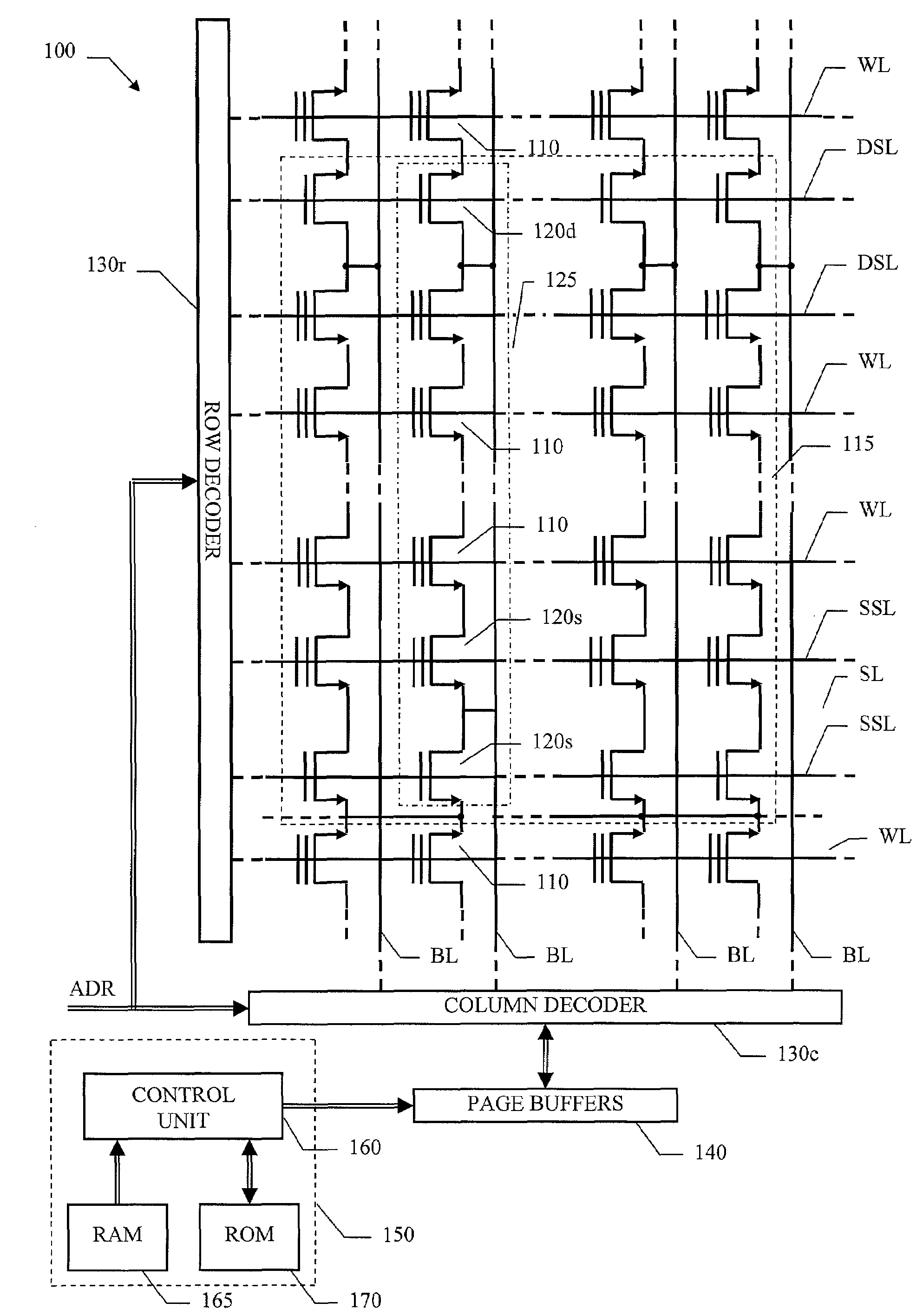
[0031]With reference in particular to FIG. 1, a non-volatile semiconductor memory device of the flash type 100 is shown. The memory device 100 includes a matrix of cells 110, typically realized by floating-gate MOS transistors; the matrix includes one or more blocks 115, each one being erasable individually.
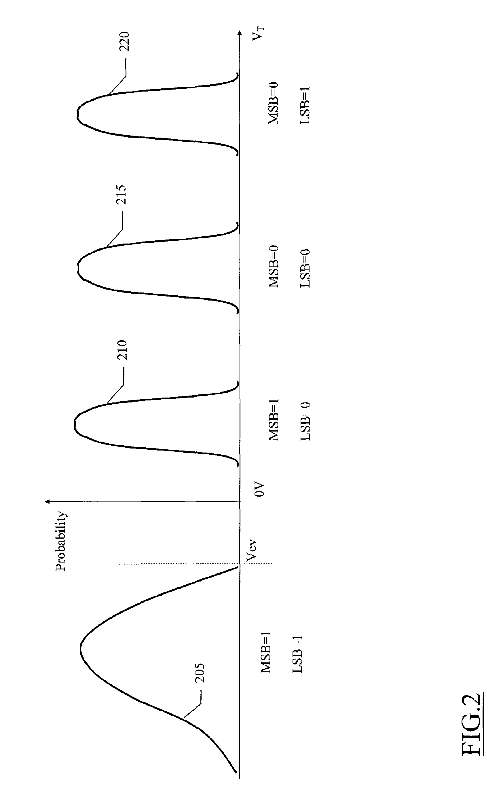
[0032]The memory device 100 is a multi-level memory, particularly (for the sake of simplicity) a four-level memory wherein each cell 110 is adapted to store a two-bit logic value comprising a Least Significant Bit (LSB) and a Most Significant Bit (MSB). More in particular, the cell 110 can be set in any one of four different states, each one associated with a corresponding logic value of the pair of bits. The state of the cell 110 is defined by its threshold voltage; in the example at issue, the threshold voltage of the cell 110 can take one of four different levels.
[0033]A typical choice (so-called Gray code) is to define the logic values corresponding to the different states of...
PUM
 Abstract
Description
Claims
Application Information