Force sensor chip

a technology of force sensor and sensor chip, which is applied in the direction of force/torque/work measurement apparatus, instruments, tension measurement, etc., can solve the problems of inability to maintain detection balance, inability to describe the thickness reduction of semiconductor substrate, and inability to reduce the thickness of semiconductor substrate, etc., to achieve favorable detection balance, increase the degree of deformation of connecting parts, and compact

Active Publication Date: 2009-05-26
HONDA MOTOR CO LTD
View PDF18 Cites 10 Cited by
  • Summary
  • Abstract
  • Description
  • Claims
  • Application Information

AI Technical Summary

Benefits of technology

[0010]It is an object of the present invention to provide, in light of the above problems, a force sensor chip in which a favorable detection balance can be maintained between the respective axial forces even when the planar shape is made compact, in which the concentration of stress in the connecting parts by applied external forces can be prevented to avoid chip damage, and in which the connecting parts can be sufficiently flexed so that the detection sensitivity can be increased while making it less likely that design errors will occur in the amounts of strain detected by the respective strain detection elements.
[0012]The thin area formed in the base member is formed to include the areas of the connecting parts. As a result, when the planar shape of the chip as such is made compact, the overall degree of deformation of the connecting parts is increased by the presence of the thin area, and the detection balance between the respective axial forces can be maintained as the chip is made more compact.
[0018]It is desirable that each of the connecting parts have a bridge part provided with an area of high rigidity, and an elastic part provided with an area of low rigidity.
[0023]The thin area formed in the base member is formed to include the areas in which the connecting parts are formed, and the degree of deformation of the connecting parts can therefore be increased. Accordingly, even if the chip is made compact in the planar direction, a favorable detection balance can be maintained between the respective axial forces as the chip is made more compact. In particular, since the boundary between the thin part of the thin area and the thick parts of other areas is formed in the supporting part and the operating part, a favorable detection balance can be maintained between the respective axial forces without affecting the connecting parts.
[0024]If the boundary of the thin area is formed in the supporting part and operating part as described above, a state of concentrated stress in the connecting parts can be avoided, and damage to the base member, i.e., to the chip, can be prevented.
[0025]Since the degree of deformation of the connecting parts overall can be increased by forming the thin area, strain can be effectively generated in the parts where deformation of the connecting parts is generated, and the detection sensitivity can be increased.

Problems solved by technology

The reason for this is that even in cases where the external forces applied in the X, Y and Z axial directions are equal, a difference is generated between the amount of deformation of the chip caused by the external forces applied in the X and Y axial directions and the amount of deformation of the chip caused by the external force applied in the Z axial direction if the planar shape alone is made more compact without varying the thickness, and it is therefore impossible to maintain the detection balance.
However, there is no description of reducing the thickness of the semiconductor substrate from the standpoint of maintaining a favorable detection balance.
Furthermore, the following problem arises in the semiconductor process when an attempt is made to reduce the entire chip to the desired thinness from the start.
Since the silicon wafer that is used to manufacture the chip is inherently thin as such in comparison with the surface area of the wafer, a further reduction in the thickness leads to a danger of warping and cracking of the wafer during the process.
However, leaving the thickness unchanged relative to the surface area of the chip makes it difficult to increase the chip sensitivity even if flexible parts are formed.
However, in this multiaxial force sensor, the problem of damage caused by the concentration of stress arises when boundaries of the thin areas (boundaries of thick parts and thin parts) are formed in the connecting parts during reduction of the thickness of the sensor chip.
There is therefore a possibility that a difference will arise between the amount of strain intended in the design and the amount of strain that is actually generated.
In other words, an unnecessary concentration of stress tends to occur, and unexpected noise is superimposed on the amount of detected strain as a result of boundaries of the thin areas being formed in the connecting parts.

Method used


Image

  • Force sensor chip
  • Force sensor chip
  • Force sensor chip

Examples


first embodiment

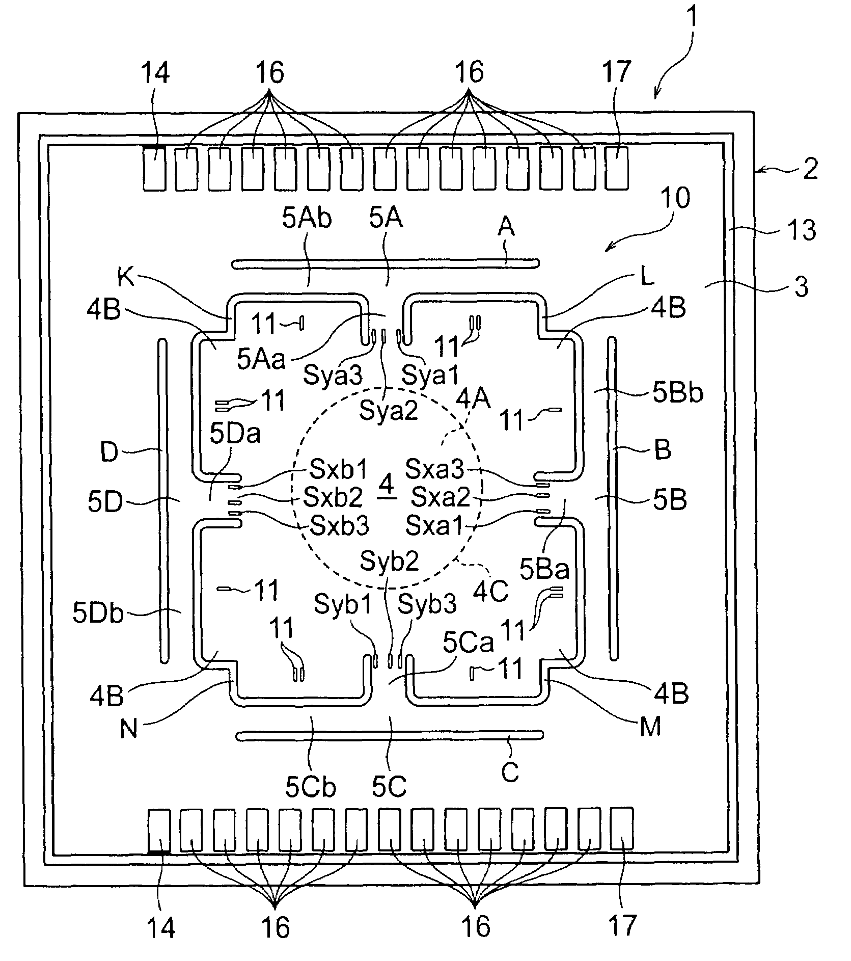
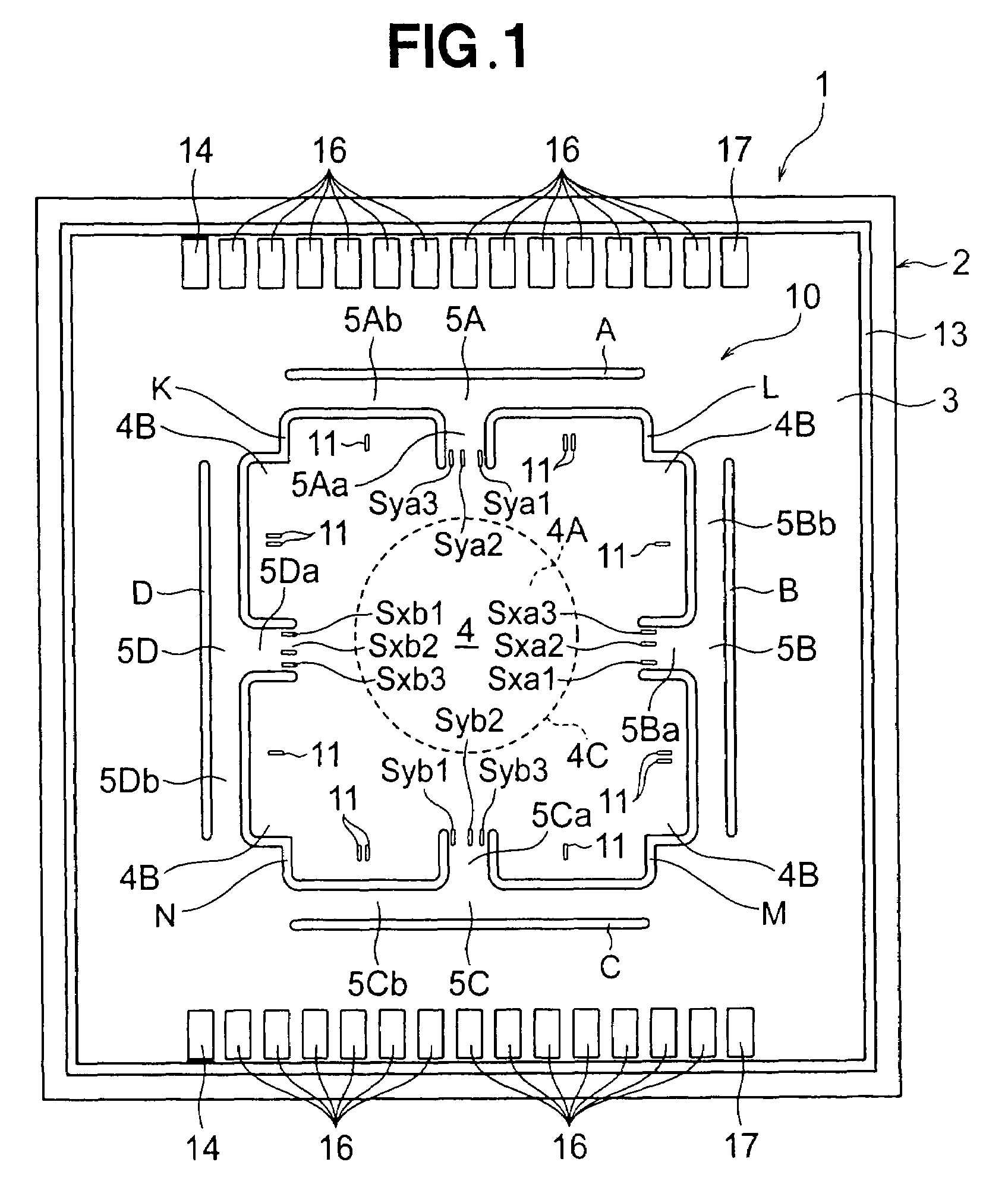
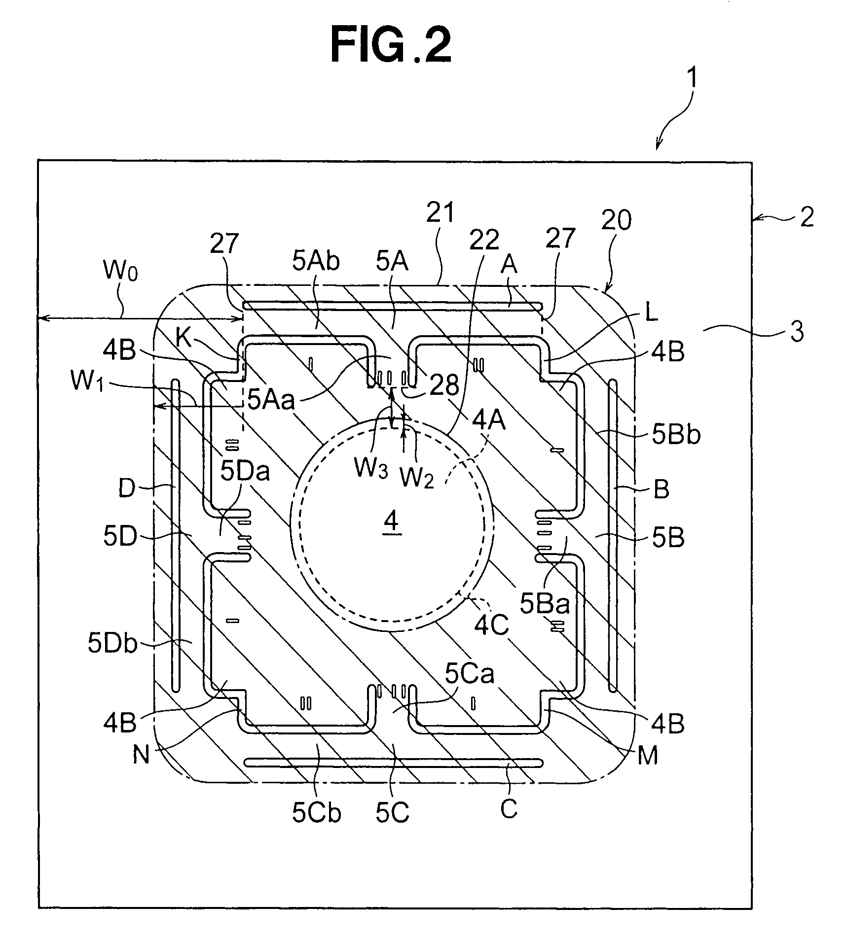
[0035]the force sensor chip of the present invention will be described with reference to FIGS. 1 through 3. In this embodiment, an example of a six-axis force sensor chip is described as a force sensor chip. The force sensor chip of the present invention is not limited to a six-axis force sensor chip.

[0036]FIG. 1 is a plan view showing the front surface of the force sensor chip. In the force sensor chip of FIG. 1, all of the strain resistance elements and temperature compensation resistance elements show a pattern comprising a plurality of holes and electrode pads.

[0037]In FIG. 1, the six-axis force sensor chip 1 of the present embodiment is formed using a semiconductor substrate which preferably has a square planar shape. For example, the length of one side of this square semiconductor substrate is 5.5 mm. The substrate is not limited to a semiconductor substrate. The six-axis force sensor chip 1 has a plate-form shape based on the semiconductor substrate.

[0038]In the six-axis forc...


PUM

PropertyMeasurementUnit
lengthaaaaaaaaaa
diameteraaaaaaaaaa
areasaaaaaaaaaa

Abstract

A force sensor chip having a multiaxial force sensing function is disclosed. The force sensor chip comprises a base member having an operating part provided with an external force application area, a supporting part for supporting the operating part, connecting parts for connecting the operating part and the supporting part, and strain resistance elements disposed in the connecting parts or within boundaries between the connecting parts and the operating part. The base member has a thin area formed with a small thickness, and the boundaries of the thin area are disposed in the supporting part and operating part.

Description

FIELD OF THE INVENTION[0001]The present invention relates to a force sensor chip and, more particularly, to a force sensor chip which has a plurality of strain resistance elements formed on the surface of a semiconductor substrate by using semiconductor manufacturing technology, and which is suitable for a six-axis force sensor or other device used as a compact force sensor in an industrial robot or the like.BACKGROUND OF THE INVENTION[0002]In automated industrial machines such as machine tools, industrial robots, and the like, forces are applied to workpieces, and the forces act from the outside because of the manner in which these machines operate. In this case, the forces and moments applied to the machines from the outside must be detected, and a control program that corresponds to these forces and moments must be performed. To ensure that a control program that corresponds to these forces and moments is carried out with a high degree of precision, the externally applied forces ...

Claims


Application Information

Patent Timeline
Patent Type & Authority Patents(United States)
IPC IPC(8): G01L1/22
CPCG01L5/162
Inventor HIRABAYASHI, YUSUKESAKURAI, NOBUHIROOHSATO, TAKESHI
Owner HONDA MOTOR CO LTD
Why Eureka
Try Eureka