

Semiconductor device and method for fabricating the same
a technology of semiconductor devices and resistors, which is applied in the direction of semiconductor devices, diodes, electrical equipment, etc., can solve the problems of gate insulation film b>104 breakdown, fluctuation in the resistance value of resistors, and so as to prevent the breakdown of mis transistors and simplify the fabrication process steps
- Summary
- Abstract
- Description
- Claims
- Application Information
AI Technical Summary
Benefits of technology
Problems solved by technology
Method used
Image

Examples
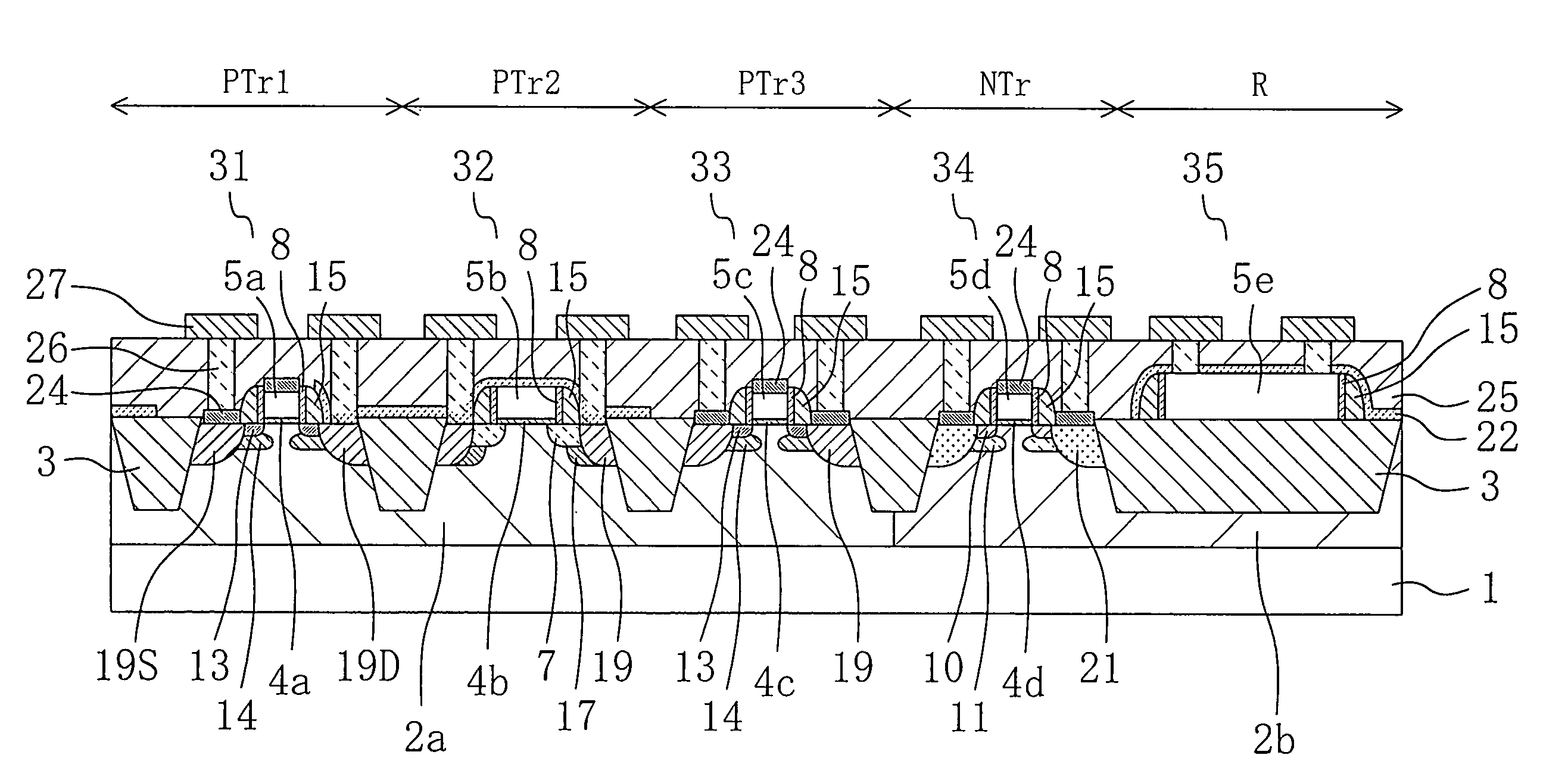
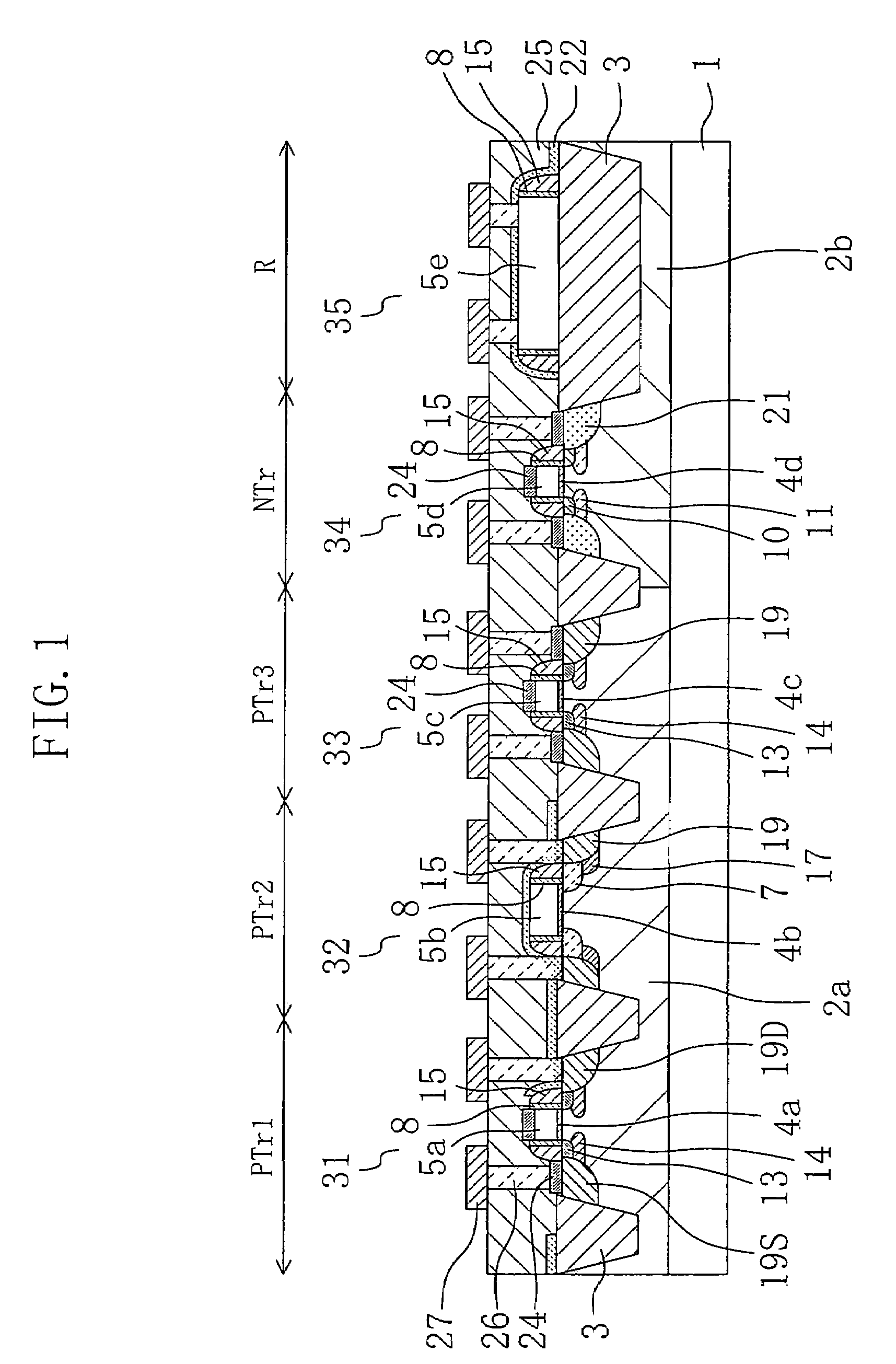
first embodiment
Modified Example of First Embodiment
[0055]Hereinafter, a modified embodiment of the first embodiment will be described with reference to the accompanying drawings. In the first embodiment, the transistors PTr1, PTr2, PTr3 and NTr are provided. In this modified example, the case where a single transistor and a resistor are provided will be described. Note that the structure of the resistor is the same as that of the first embodiment and therefore the illustration and description thereof will be omitted.
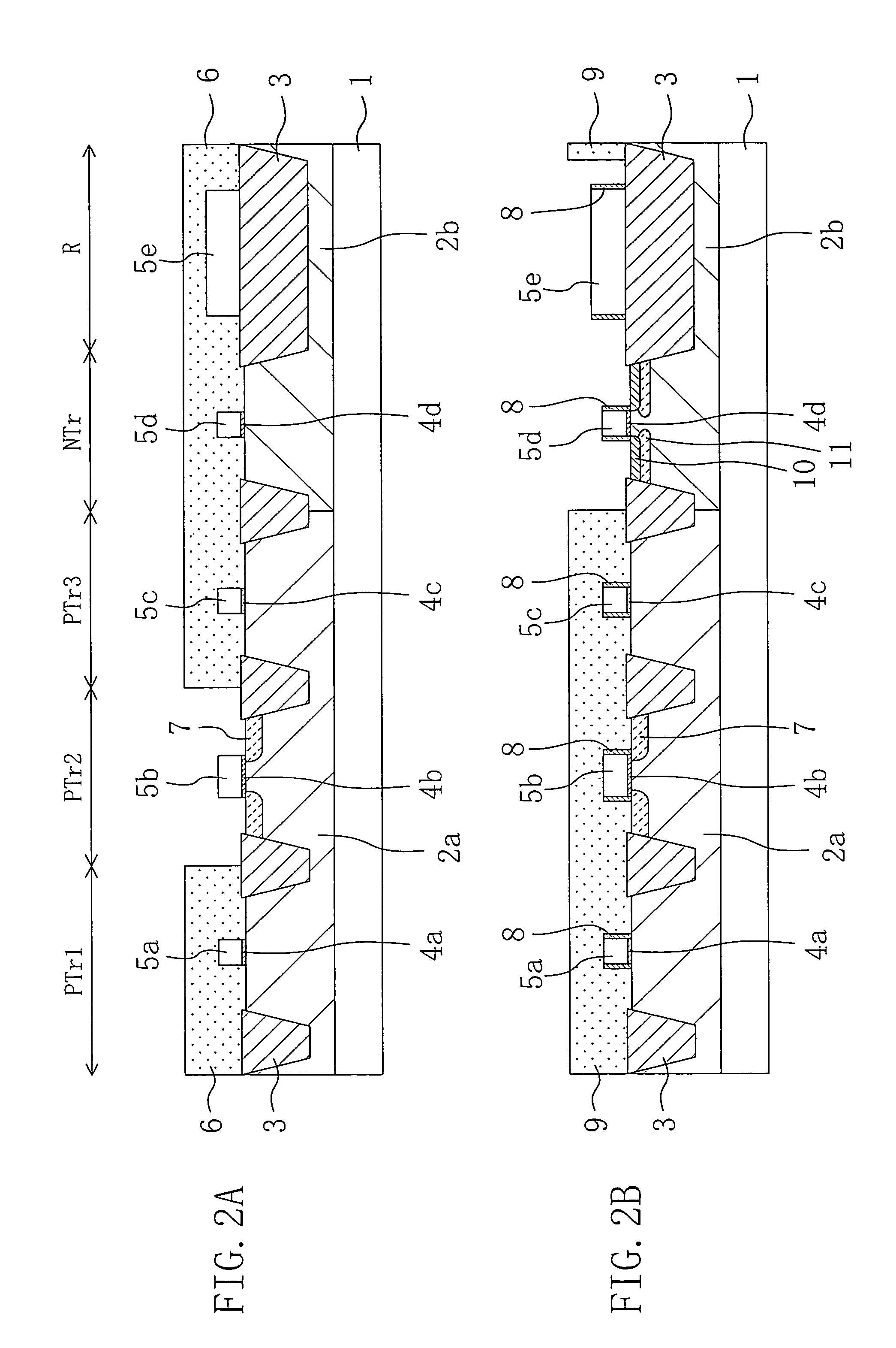
[0056]According to fabrication process steps according to this modified example, in the same process steps as those of FIGS. 2A through 5A in the first embodiment, a gate insulation film 4aa and a gate electrode 5aa are formed on the active region 30 surrounded by the isolation region 3 shown in FIG. 7A, and then, a p-type lightly doped layer 13, an n-type pocket doped layer 14, a first sidewall 8, a second sidewall 15 and a p-type heavily doped layer 19 are formed in this order. In FI...
PUM
 Abstract
Description
Claims
Application Information