Mask pattern generating method

a technology of mask pattern and generating method, which is applied in the direction of photo-taking process, photomechanical apparatus, instruments, etc., can solve the problems of difficult to transfer the pattern to the photoresist film in such a manner, product yield and product reliability may be reduced, and desired transistor characteristics may not be easily obtained. achieve the effect of improving product yield and product reliability

Inactive Publication Date: 2009-06-02
SONY CORP
View PDF10 Cites 35 Cited by
  • Summary
  • Abstract
  • Description
  • Claims
  • Application Information

AI Technical Summary

Benefits of technology

[0021]As described above, when a semiconductor device is manufactured, it may be difficult to perform patterning with high precision in such a manner as to correspond to the design pattern, so that product yield and product reliability may be decreased.
[0022]Accordingly, it is desirable to provide a mask pattern forming method that can improve product yield and product reliability.
[0025]According to an embodiment of the present invention, it is possible to provide a mask pattern forming method that can improve product yield and product reliability.

Problems solved by technology

However, when pattern transfer is performed as described above, it can be difficult to transfer the pattern to the photoresist film in such a manner as to correspond to a desired design pattern.
Therefore desired transistor characteristics may not be obtained easily.
As described above, when a semiconductor device is manufactured, it may be difficult to perform patterning with high precision in such a manner as to correspond to the design pattern, so that product yield and product reliability may be decreased.

Method used


Image

  • Mask pattern generating method
  • Mask pattern generating method
  • Mask pattern generating method

Examples


Embodiment Construction

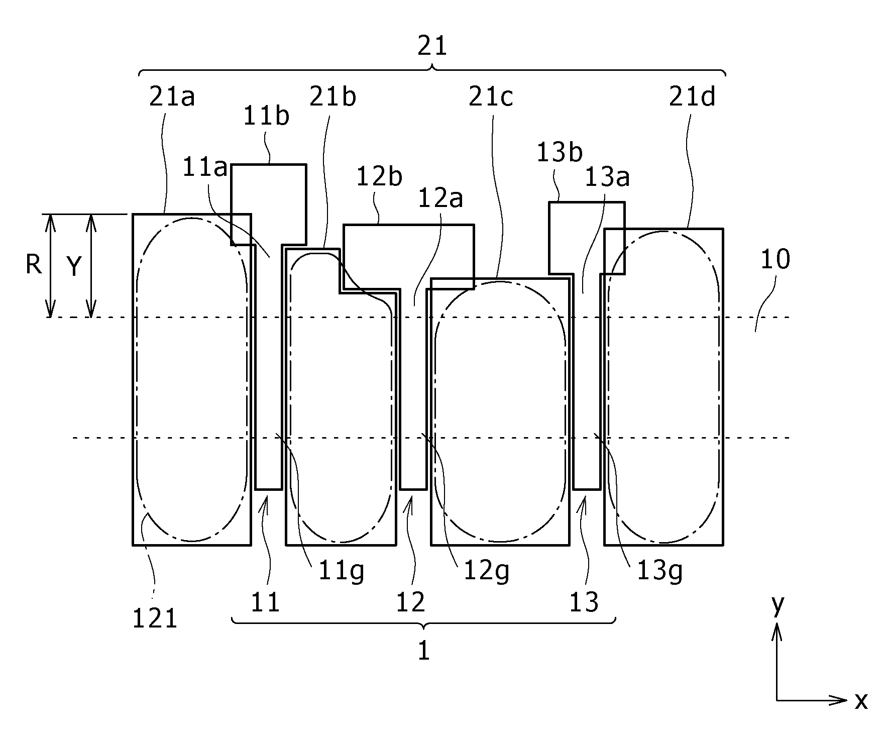
[0040]An embodiment of the present invention will be described.

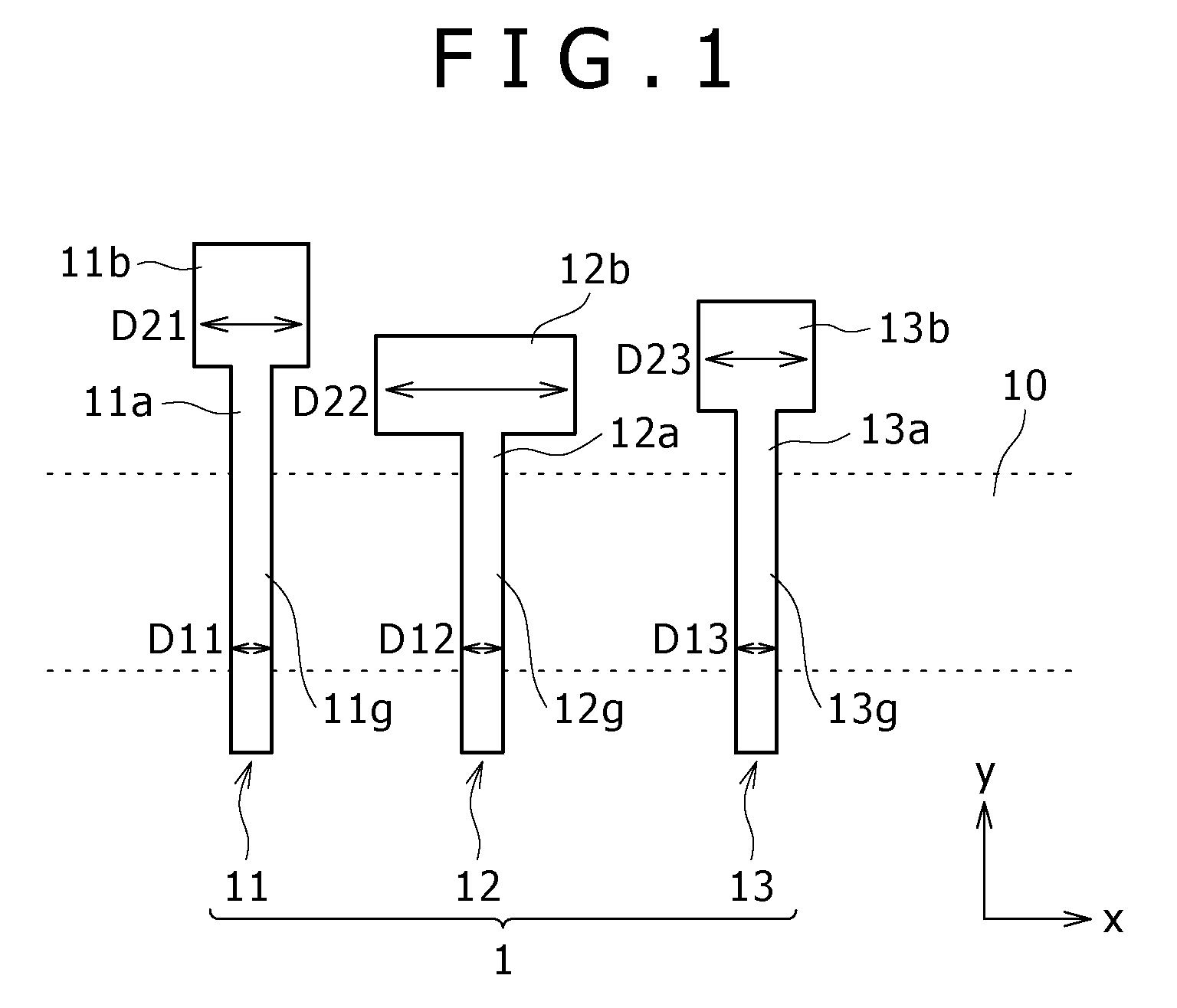
[0041]FIG. 1 is a plan view showing a design pattern of a patterned conductive layer in the embodiment of the present invention.

[0042]In the present embodiment, as shown in FIG. 1, a first conductive layer 11, a second conductive layer 12, and a third conductive layer 13 are patterned as a conductive layer 1.

[0043]In this case, as shown in FIG. 1, the conductive layer 1 is formed by patterning the first conductive layer 11, the second conductive layer 12, and the third conductive layer 13 such that the first conductive layer 11, the second conductive layer 12, and the third conductive layer 13 include gate electrodes 11g, 12g, and 13g, first extension parts 11a, 12a, and 13a, and second extension parts 11b, 12b, and 13b, respectively.

[0044]Specifically, as shown in FIG. 1, the gate electrodes 11g, 12g, and 13g extend in a y-direction orthogonal to an x-direction in which an active region 10 extend on a wafer surface, the...


PUM

PropertyMeasurementUnit
conductiveaaaaaaaaaa
photosensitiveaaaaaaaaaa
phaseaaaaaaaaaa

Abstract

Disclosed herein is a mask pattern generating method for generating a mask pattern to be formed in a Levenson phase shift mask used in a light exposure process for exposing a photoresist film formed on a fabricated film to be patterned into a conductive layer to light when the conductive layer is patterned by photolithography, the conductive layer including a gate electrode formed in an active region extending in a first direction in a wafer in such a manner as to extend in a second direction orthogonal to the first direction, the mask pattern generating method including: a phase shifter arranging step; a shifter pattern image obtaining step; a trim pattern image obtaining step; and a phase shifter elongating step.

Description

CROSS REFERENCES TO RELATED APPLICATIONS[0001]The present invention contains subject matter related to Japanese Patent Application JP 2006-114827 filed in the Japan Patent Office on Apr. 18, 2006, the entire contents of which being incorporated herein by reference.BACKGROUND OF THE INVENTION[0002]1. Field of the Invention[0003]The present invention relates to a mask pattern generating method, and particularly to a mask pattern generating method for generating a mask pattern for a Levenson phase shift mask used when a conductive layer having gate electrodes is patterned by photolithography.[0004]2. Description of the Related Art[0005]When a semiconductor device is manufactured, a fine pattern is formed on a wafer by photolithography.[0006]In this case, first, a photoresist film of a photosensitive material is formed on a surface of a fabricated film formed on the wafer. Thereafter a photomask having a mask pattern formed therein is illuminated, whereby a mask pattern image produced b...

Claims


Application Information

Patent Timeline
Patent Type & Authority Patents(United States)
IPC IPC(8): G03C5/00G03F9/00G03F1/30G03F1/68G03F1/70H01L21/027H01L21/82
CPCG03F1/30H01L21/0274H01L21/32139G03F1/70
Inventor OGAWA, KAZUHISANAKAMURA, SATOMINAKAYAMA, KOHICHI
Owner SONY CORP
Why Eureka
Try Eureka