Structure of package on package and method for fabricating the same

a technology of packaging and structure, applied in the direction of semiconductor devices, semiconductor/solid-state device details, electrical apparatus, etc., can solve the problems of difficult to dispose vias, small volume of packaging on packages, and the size of mother boards is not increased or even reduced, so as to increase the space for wiring layout

Active Publication Date: 2009-06-23
ADVANCED SEMICON ENG INC
View PDF3 Cites 128 Cited by
  • Summary
  • Abstract
  • Description
  • Claims
  • Application Information

AI Technical Summary

Benefits of technology

[0009]The invention is directed to a structure of a package on package and a method for fabricating the same. Packages are connected by pins so as to increase the space for wiring layout.

Problems solved by technology

Also, the package on package has small volume due to stacked structure.
Therefore, the size of the mother board is not increased or even reduced.
Therefore, it is difficult to dispose vias when the circuits have to be disposed on inner layers.
It is even more difficult to disposes the circuits in the high-density area adjacent to the chip 18.

Method used


Image

  • Structure of package on package and method for fabricating the same
  • Structure of package on package and method for fabricating the same
  • Structure of package on package and method for fabricating the same

Examples


first embodiment

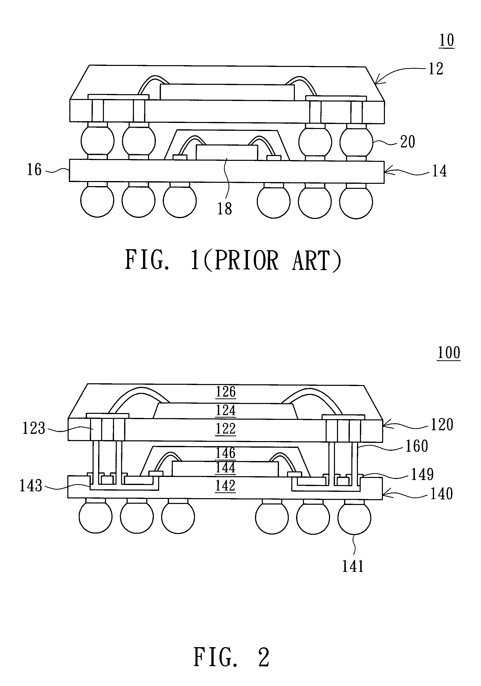
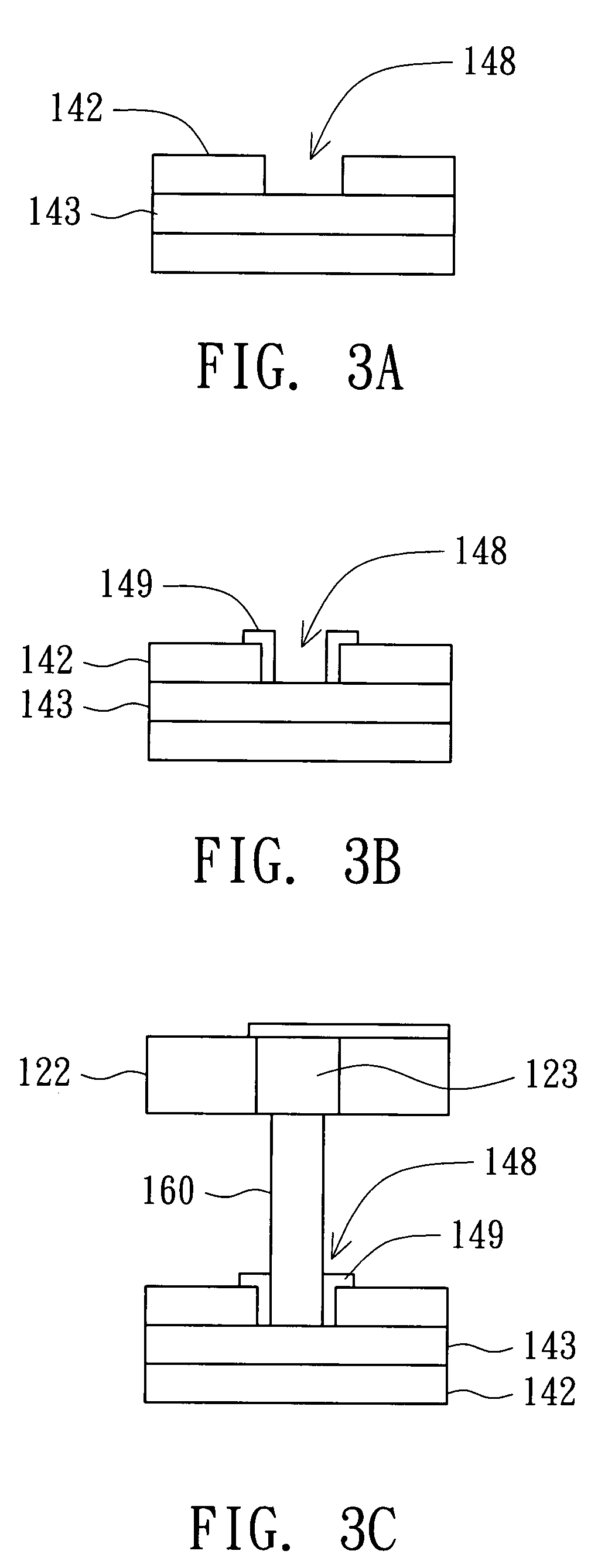
[0020]Please referring to FIG. 2, illustrating a structure of a package on package according to a first embodiment of the present invention. The package on package 100 of the present embodiment includes a first package 120, a second package 140 and a plurality of pins 160. The first package 120 includes a first substrate 122 and a first chip 124 disposed on the first substrate 122. The first package 120 further includes a first inner circuit 123 and a first molding material 126. The first inner circuit 123 is formed in the first substrate 122. The first chip 124 and the first inner circuit 123 are electrically connected together. The first molding material 126 encapsulates at least a portion of the first substrate 122 and the first chip 124.

[0021]The second package 140 includes a second substrate 142 and a second chip 144 disposed on the second substrate 142. The second package 140 is disposed under the first package 120. The second package 140 further includes a second inner circui...

second embodiment

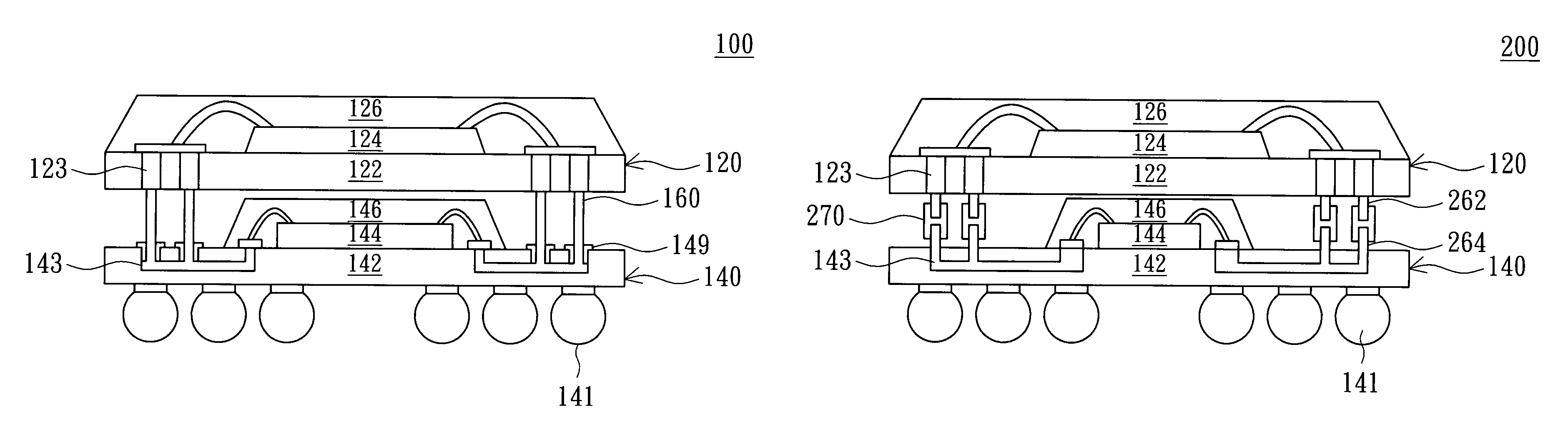
[0030]The present embodiment and the above embodiment are only different in the connection of the first package and the second package. The same parts are not described redundantly. Please referring to FIG. 4, the structure of the package on package according to a second embodiment of the present invention is illustrated in FIG. 4. The package on package 200 of the present embodiment includes the first package 120, the second package 140, a plurality of first pins 262, a plurality of second pins 264 and a connecting component 270. The first pins 262 are disposed on the first package 120. Preferably, the first pins 262 are disposed on the lower surface of the first substrate 122 and electrically connected with the first inner circuit 123. The second pins 264 are disposed on the second package 140. Preferably, the second pins 264 are disposed on the upper surface of the second substrate 140 and electrically connected with the second inner circuit 143.

[0031]The connecting component 270...


PUM


Abstract

A structure of a package on package and a method for fabricating the same are provided. The structure of the package on package includes a first package, a second package and a plurality of pins. The first package includes a first substrate and a first chip disposed thereon. The second package includes a second substrate and a second chip disposed thereon. The second package is disposed under the first package. The second package includes a plurality of holes. The pins are disposed on the first package and inserted to the holes so as to electrically connect the first package and the second package.

Description

[0001]This application claims the benefit of Taiwan application Serial No. 095139858, filed Oct. 27, 2006, the subject matter of which is incorporated herein by reference.BACKGROUND OF THE INVENTION[0002]1. Field of the Invention[0003]The invention relates in general to a structure of a package on package and a method for fabricating the same, and more particularly to a structure of a package on package connected by pins and a method for fabricating the same.[0004]2. Description of the Related Art[0005]As portable multimedia devices become more and more popular, the trend toward new storage structures with higher digital signal processing, larger storage capacity and more flexibility grows accordingly. Therefore, the application of stacked package on package (PoP) extends rapidly.[0006]The package on package is a new three-dimensional packaging technology with lowest cost for logic and memory Integration. The stacked package on package is used for developing devices with new appeara...

Claims


Application Information

Patent Timeline
Patent Type & Authority Patents(United States)
IPC IPC(8): H01L23/02
CPCH01L23/3128H01L25/105H01L25/50H01L2224/48091H01L2224/48227H01L2924/15192H01L2924/15311H01L2924/00014H01L24/48H01L2225/1023H01L2225/1058H01L2924/181H01L2924/00012H01L2224/45099H01L2224/45015H01L2924/207
Inventor CHOU, CHE-YACHIU, CHI-TSUNG
Owner ADVANCED SEMICON ENG INC
Why Eureka
Try Eureka