Nonvolatile memory device and related programming method

a technology of nonvolatile memory and programming method, which is applied in the direction of static storage, digital storage, instruments, etc., can solve the problems of troublesome users, lost stored data of volatile semiconductor memory devices, and traditionally difficult for users to update the data stored

Active Publication Date: 2009-06-23
SAMSUNG ELECTRONICS CO LTD
View PDF12 Cites 51 Cited by
  • Summary
  • Abstract
  • Description
  • Claims
  • Application Information

AI Technical Summary

Problems solved by technology

However, unlike nonvolatile semiconductor memory devices, volatile semiconductor memory devices lose stored data when disconnected from an external power source.
As a result, nonvolatile semiconductor memory devices are often used to store data in electronic devices where power is limited or may be unexpectedly cut off.
Unfortunately, it has traditionally been difficult for users to update data stored in MROM, PROM, and EPROM due at least in part to difficulties in performing erase operations.
Unfortunately, as a result, the effective load capacitance for each memory cell connected to a word line may vary significantly in accordance with its location along the word line.
This results proves troubling since the effective load capacitance may affect the timing of the program word line voltages apparent at different memory cells.
Due to these load capacitance effects, program operations in conventional NAND flash memory devices may be limited by the timing requirements of memory cells located furthest from row decoder circuit 120.
However, timing requirements such as these may significantly impair the overall operational performance of NAND flash memory devices.

Method used


Image

  • Nonvolatile memory device and related programming method
  • Nonvolatile memory device and related programming method
  • Nonvolatile memory device and related programming method

Examples


Embodiment Construction

[0040]Exemplary embodiments of the invention are described below with reference to the corresponding drawings. These embodiments are presented as teaching examples. The actual scope of the invention is defined by the claims that follow.

[0041]Briefly, selected embodiments of the invention provide nonvolatile memory devices and related programming methods wherein a duration with which a program word line voltage is applied to a selected word line is adjusted in successive program loops according to whether a memory cell located furthest from a row decoder circuit along the selected word line has been successfully programmed. By adjusting this duration, the reliability and performance of nonvolatile memory devices according to selected embodiments of the invention are improved relative to conventional nonvolatile memory devices.

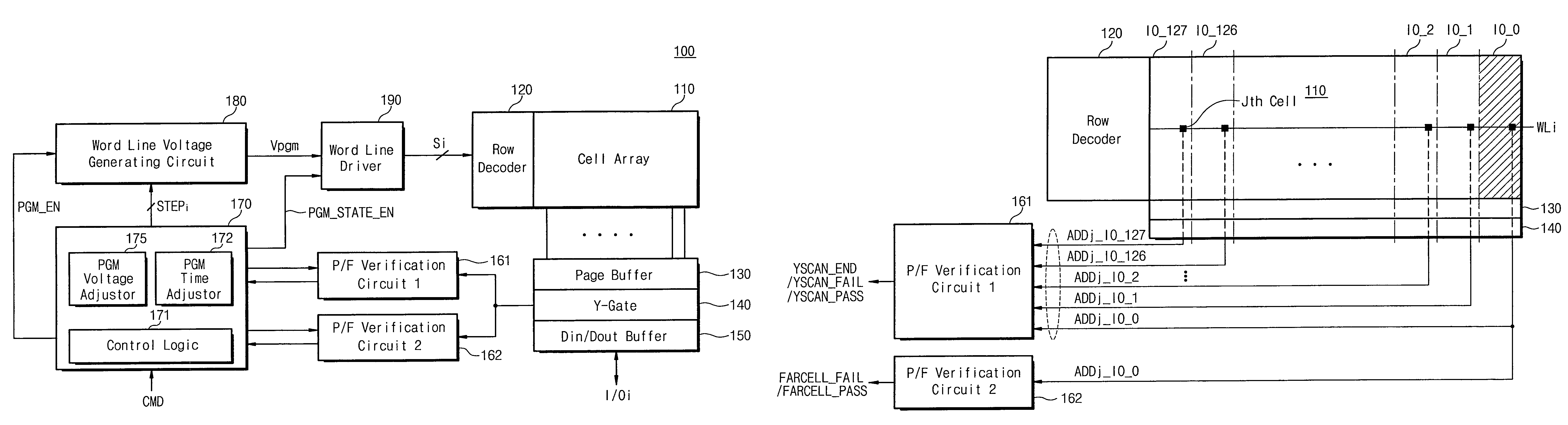
[0042]FIG. 3 is a block diagram of a nonvolatile memory device 100 according to one embodiment of the present invention. For explanation purposes, it will be as...


PUM


Abstract

In a nonvolatile memory device, a first verification result indicates whether a block of memory cells has been successfully programmed and a second verification result indicates whether a far cell in the block has been is successfully programmed. A controller defines the level and application time for the program voltage applied during a next program loop in response to the first and second verification results.

Description

BACKGROUND OF THE INVENTION[0001]1. Field of the Invention[0002]Embodiments of the invention relate generally to nonvolatile memory devices. More particularly, embodiments of the invention relate to nonvolatile memory devices and related programming methods having improved performance relative to conventional nonvolatile memory devices and programming methods.[0003]A claim of priority is made to Korean Patent Application No. 2006-22789, filed on Mar. 10, 2006, the disclosure of which is hereby incorporated by reference in its entirety.[0004]2. Description of Related Art[0005]Semiconductor memory devices can be roughly divided into two categories including volatile semiconductor devices and nonvolatile semiconductor memory devices. Volatile semiconductor memory devices tend to have faster read and write times than nonvolatile semiconductor memory devices. However, unlike nonvolatile semiconductor memory devices, volatile semiconductor memory devices lose stored data when disconnected...

Claims


Application Information

Patent Timeline
Patent Type & Authority Patents(United States)
IPC IPC(8): G11C16/06
CPCG11C16/0483G11C16/3454G11C16/3459G11C16/10
Inventor PARK, MIN-GUNJO, SUNG-JYU
Owner SAMSUNG ELECTRONICS CO LTD
Why Eureka
Try Eureka