Handlers for testing semiconductor devices that are capable of maintaining stable temperature in test environments

a technology of test environment and handler, which is applied in the direction of individual semiconductor device testing, semiconductor/solid-state device testing/measurement, instruments, etc., can solve the problems of increasing the number of semiconductor memory devices, increasing the heat generation of semiconductor devices, and the conventional handler of semiconductor devices cannot maintain a constant inner temperature of the test chamber, so as to achieve the effect of minimizing temperature variation

Active Publication Date: 2009-06-30
SAMSUNG ELECTRONICS CO LTD
View PDF21 Cites 16 Cited by
  • Summary
  • Abstract
  • Description
  • Claims
  • Application Information

AI Technical Summary

Benefits of technology

[0013]Example embodiments provide semiconductor device test handlers that may maintain a stable temperature or temperatures in a test environment by, for example, partitioning a test chamber into two or more test spaces, installing first and / or second chambers for temperature control in each of the partitioned test spaces, and / or performing a temperature control operation on the test chambers using a temperature-control medium.
[0022]The de-soak chamber may be disposed above or below the soak chamber (i.e., in the same direction as the soak chamber) to minimize a temperature variation that may be generated in the test chamber while the test-completed test tray is moved or test trays are moved.

Problems solved by technology

However, it is difficult to increase the number of semiconductor memory devices when the increase is applied to the handler as well as to the tester.
The conventional handler for the semiconductor device cannot maintain a constant inner temperature of a test chamber when the number of semiconductor devices tested inside the test chamber during a parallel test increases.
However, as high-speed semiconductor devices develop, more heat is generated from the semiconductor devices themselves during an electrical test.

Method used


Image

  • Handlers for testing semiconductor devices that are capable of maintaining stable temperature in test environments
  • Handlers for testing semiconductor devices that are capable of maintaining stable temperature in test environments
  • Handlers for testing semiconductor devices that are capable of maintaining stable temperature in test environments

Examples


Embodiment Construction

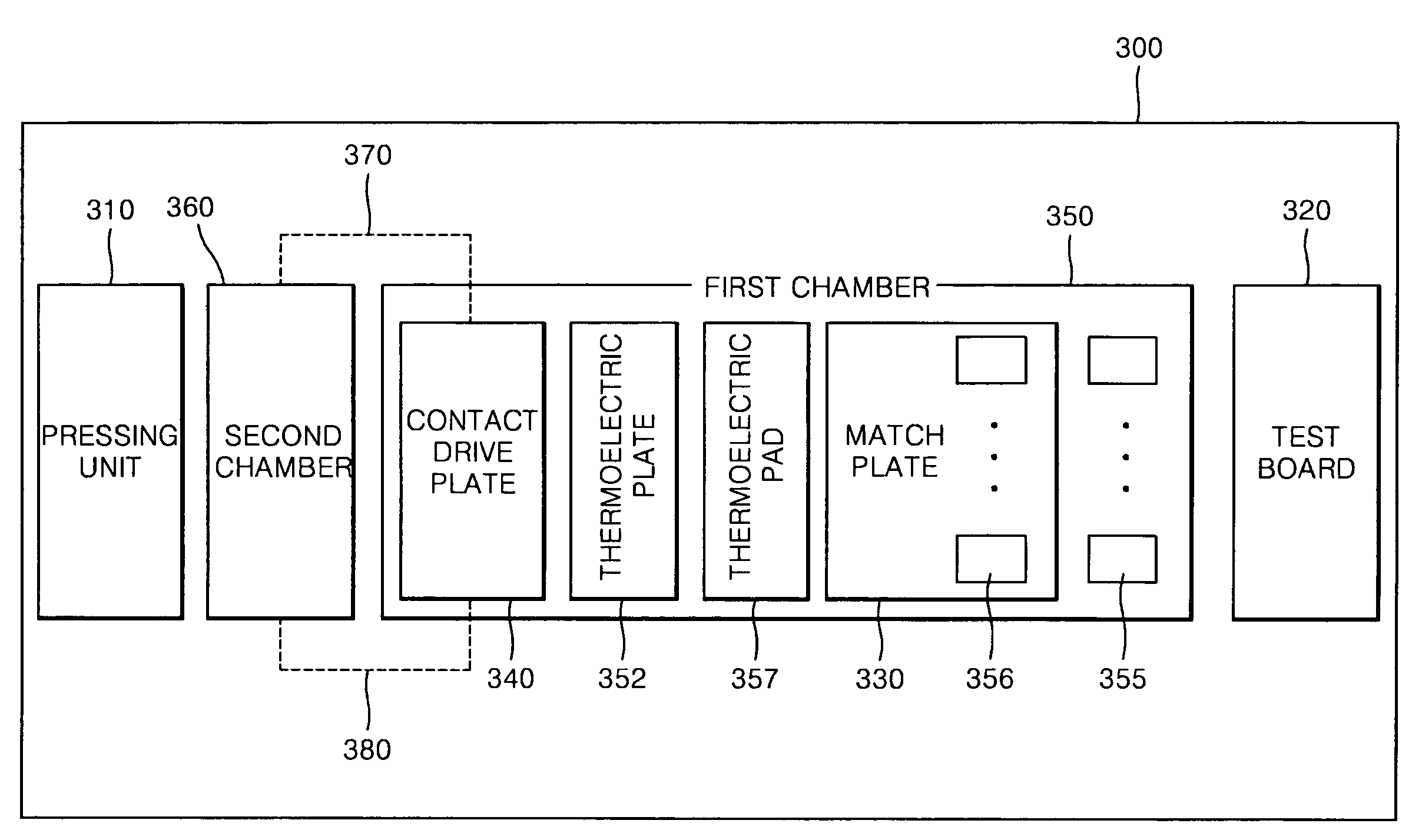
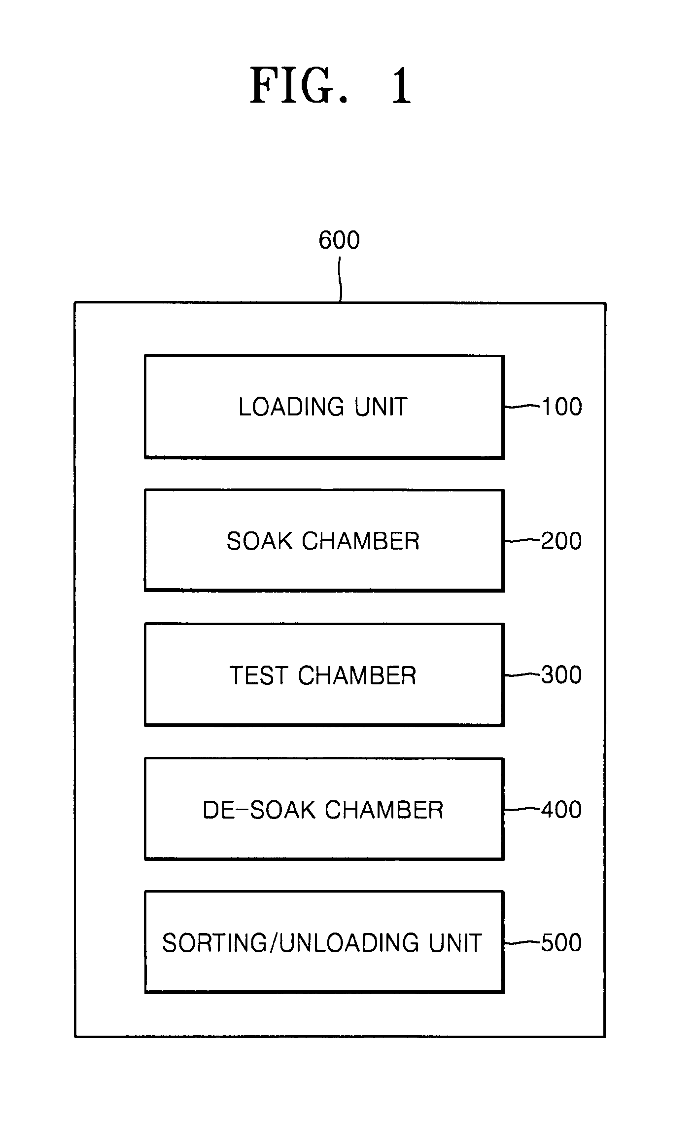
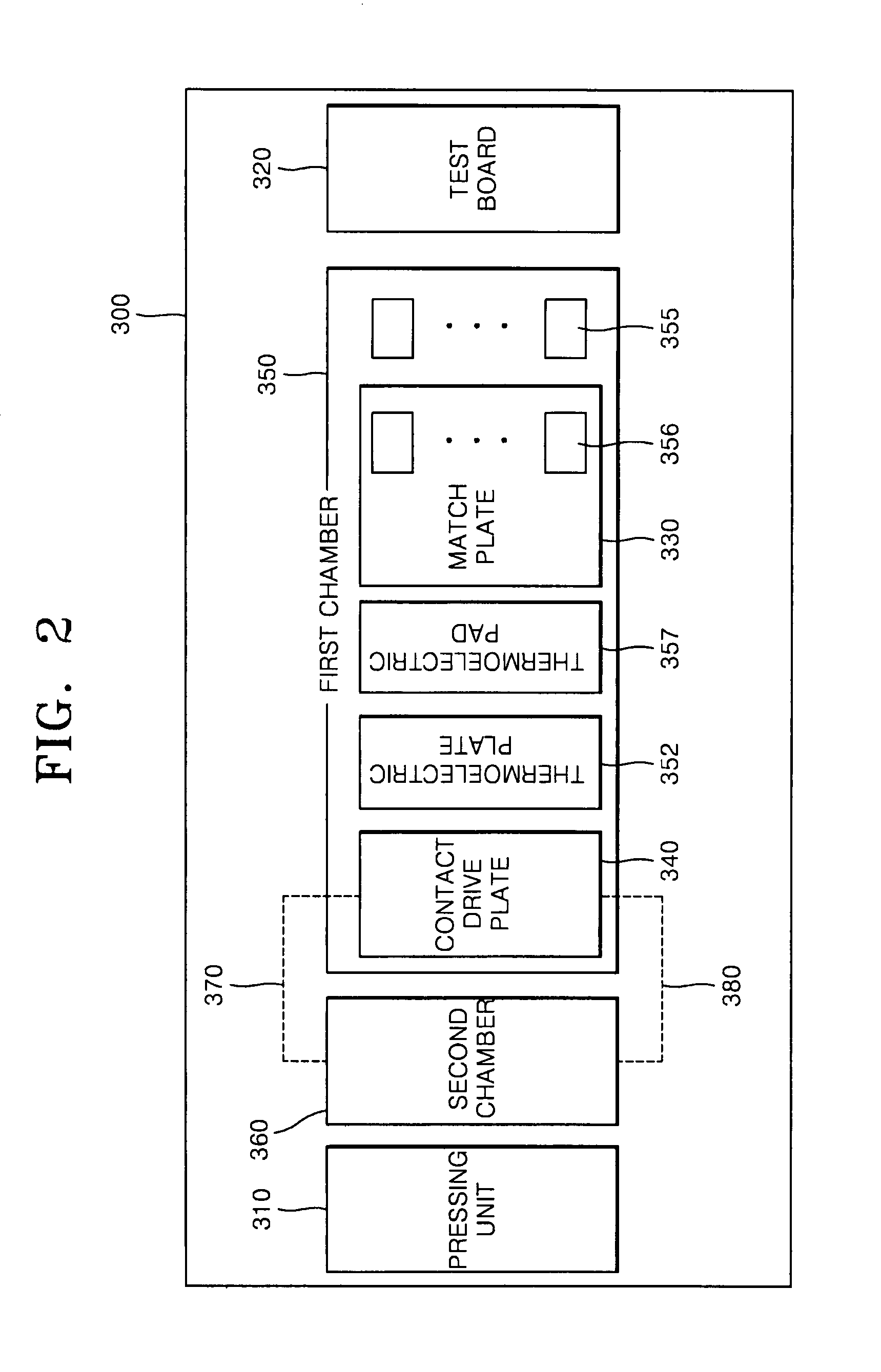
[0032]Example embodiments will now be described more fully with reference to the accompanying drawings. Embodiments, however, may be embodied in many different forms and should not be construed as being limited to the example embodiments set forth herein. Rather, these example embodiments are provided so that this disclosure will be thorough and complete, and will fully convey the scope to those skilled in the art. In the drawings, the thicknesses of layers and regions may be exaggerated for clarity.

[0033]It will be understood that when a component is referred to as being “on,”“connected to,” or “coupled to” another component, it may be directly on, connected to, or coupled to the other component or intervening components may be present. In contrast, when a component is referred to as being “directly on,”“directly connected to,” or “directly coupled to” another component, there are no intervening components present. As used herein, the term “and / or” includes any and all combinations...


PUM


Abstract

A semiconductor device test handler for maintaining stable temperature in a test environment may include a loading unit that loads a plurality of semiconductor devices mounted on a test tray; a soak chamber configured to receive the test tray from the loading unit and to age the semiconductor devices at an aging temperature; and a test chamber configured to receive and test the aged semiconductor devices. The test chamber may include: a test board; a first chamber; a second chamber; one or more pipelines connected to the first and second chambers that allow a temperature-control medium to flow between the first and second chambers; a de-soak chamber that further ages the tested semiconductor devices so that the tested semiconductor devices substantially return to ambient temperature; and a sorting and unloading unit that sorts the tested semiconductor devices according to results of the test and that unloads the sorted semiconductor devices.

Description

PRIORITY STATEMENT[0001]This application claims priority from Korean Patent Application No. 10-2006-0032743, filed on Apr. 11, 2006, in the Korean Intellectual Property Office (KIPO), the entire contents of which are incorporated herein by reference.BACKGROUND[0002]1. Field[0003]Example embodiments relate to electrical test apparatuses for semiconductor devices. Also, example embodiments relate to handlers (i.e., test robots) that electrically connect semiconductor devices to testers and automatically perform loading, testing, sorting, and / or unloading operations on the semiconductor devices.[0004]2. Description of Related Art[0005]A handler used for an electrical test of a semiconductor device is a kind of automatic test robot loading a semiconductor device, automatically performing an electrical test by electrically connecting the loaded semiconductor device to a tester, sorting semiconductor devices according to the results of the electrical test, and unloading sorted semiconduct...

Claims


Application Information

Patent Timeline
Patent Type & Authority Patents(United States)
IPC IPC(8): G01R31/02
CPCG01R31/2865G01R31/2862G01R31/26H01L22/00
Inventor KANG, SEONG-GOOLEE, JUN-HOKANG, KI-SANGSHIM, HYUN-SEOPKAM, DO-YOUNGLEE, JAE-ILKANG, JU-IL
Owner SAMSUNG ELECTRONICS CO LTD
Why Eureka
Try Eureka