Method of manufacturing a microlens substrate comprising pressure-joining a substrate to a base material in a state that the base material is heated while cooling the other major surface of the base material

a manufacturing method and technology of a microlens substrate, which are applied in the direction of glass tempering devices, instruments, manufacturing tools, etc., can solve the problems of complex manufacturing process, inability to obtain sufficient light resistance of a manufactured microlens substrate, and difficulty in obtaining a microlens substrate having sufficient durability in the case of using such a method. , to achieve the effect of excellent durability

Inactive Publication Date: 2009-06-30
SEIKO EPSON CORP
View PDF10 Cites 2 Cited by
  • Summary
  • Abstract
  • Description
  • Claims
  • Application Information

AI Technical Summary

Benefits of technology

[0009]It is one object of the invention to provide a method of manufacturing a microlens substrate which makes it possible to easily manufacture a microlens substrate having excellent optical characteristics and durability.

Problems solved by technology

However, since an uncured resin material is used to manufacture a microlens substrate, it has been difficult to obtain a microlens substrate having sufficient durability in the case of using such a method.
In particular, since deterioration or the like of the resin material tends to be generated due to light having a small wavelength in a photocuring resin material used in the 2P method, there is a possibility that sufficient light resistance of a manufactured microlens substrate cannot be obtained.
For example, a step of aligning the cover glass or the like is required in such a method, and therefore, the manufacturing process has been complicated.
Thus, although an appropriate cleaning process is required, there is a possibility that such a cleaning process results in deterioration or the like of the resin material constituting the resin layer.
As a result, there is a possibility that the quality of the manufactured microlens substrate is lowered and this results in lowering of a yield rate of manufacturing the microlens substrates.

Method used


Image

  • Method of manufacturing a microlens substrate comprising pressure-joining a substrate to a base material in a state that the base material is heated while cooling the other major surface of the base material
  • Method of manufacturing a microlens substrate comprising pressure-joining a substrate to a base material in a state that the base material is heated while cooling the other major surface of the base material
  • Method of manufacturing a microlens substrate comprising pressure-joining a substrate to a base material in a state that the base material is heated while cooling the other major surface of the base material

Examples


example

Example 1

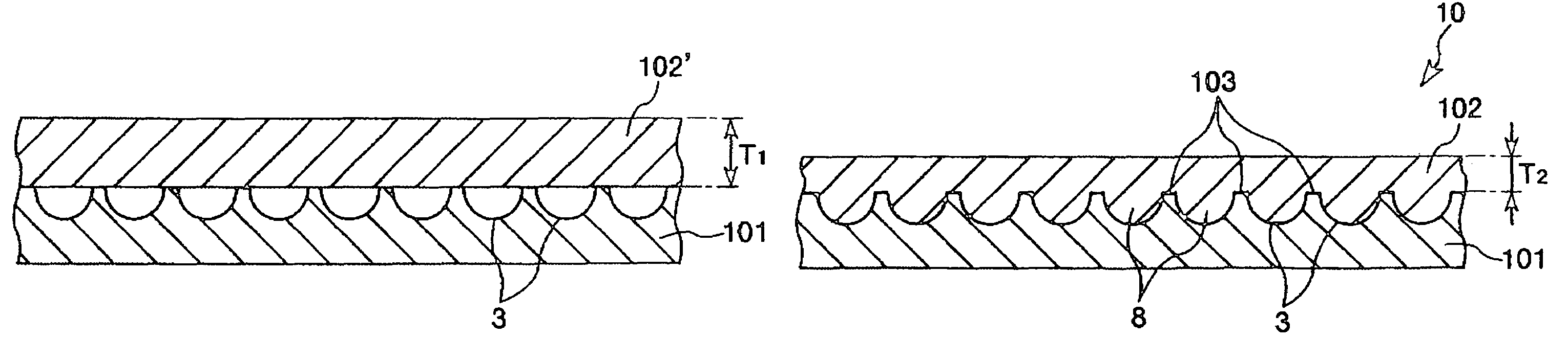
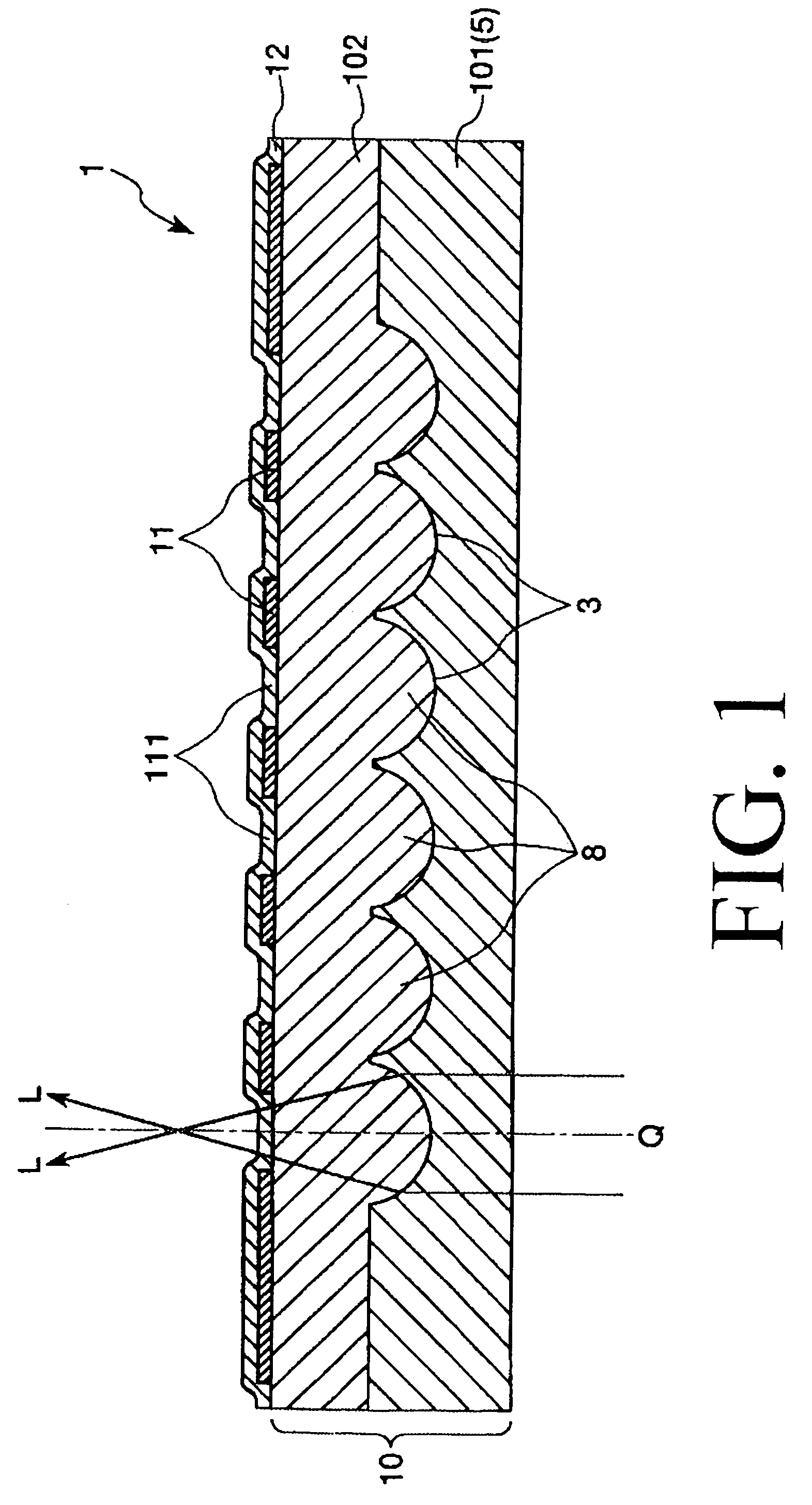
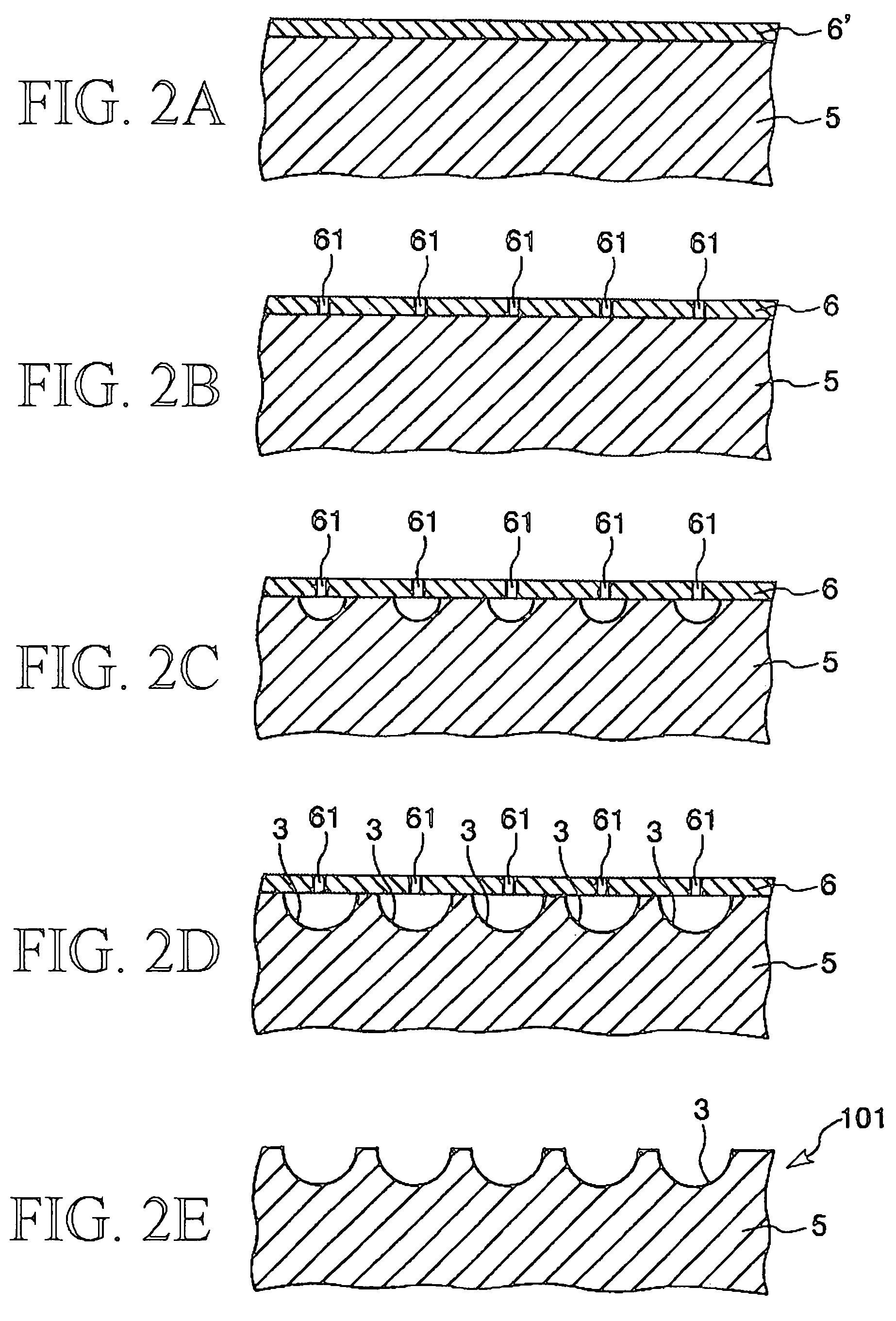
[0161]A substrate with concave portions for microlenses equipped with a plurality of concave portions was manufactured, and then a microlens substrate was manufactured using the substrate with concave portions for microlenses in the following manner.

[0162]

[0163]First, a quartz glass substrate (which has a glass transformation point of 1060° C. and an index of refraction of 1.46) having a thickness of 2.0 mm was prepared as a glass substrate.

[0164]The quartz glass substrate was soaked in a cleaning liquid (that is, a mixture of 80% sulfuric acid solution and 20% hydrogen peroxide solution) heated to 85° C. to be washed, thereby cleaning its surface.

[0165]Next, Cr films each having a thickness of 0.03 μm were formed on the quartz glass substrate by means of a spattering method. Namely, a mask and a rear face protective film formed both of the Cr films were formed on the both major surfaces of the quartz glass substrate.

[0166]Next, a laser machining was carried out with respec...

example 2

[0178]A microlens substrate was manufactured using a substrate with concave portions obtained in the same manner as that in Example 1 described above as follows.

[0179]

[0180]A thin glass substrate (glass substrate) having a glass transformation point of 660° C. and an index of refraction of 1.61 was prepared. The thickness T1 of the glass substrate was 0.5 mm.

[0181]The glass substrate was mounted on the substrate with concave portions so as to face one major surface of the substrate with concave portions on which the concave portions were formed (see FIG. 3(a)).

[0182]Next, after reducing the ambient pressure to 5 Pa, the substrate with concave portions and the thin glass substrate were heated at 800° C. In this case, they were heated while cooling the major surface of the thin glass substrate opposite to the major surface thereof on which the substrate with concave portions was mounted.

[0183]Next, the thin glass substrate was pressure-joined to the substrate with concave portions, wh...


PUM

PropertyMeasurementUnit
thicknessaaaaaaaaaa
thicknessaaaaaaaaaa
depthaaaaaaaaaa

Abstract

A method of manufacturing a microlens substrate having a plurality of microlenses includes the steps of: preparing a substrate having two major surfaces and a plurality of concave portions formed in one of the two major surfaces, each of the concave portions having a shape corresponding to that of each of the microlenses being formed in the one of the two major surfaces of the substrate; preparing a base material substrate formed of glass having a transformation point lower than that of a constituent material constituting the substrate; and pressure-joining the substrate to the base material substrate in a heating state. In the pressure-joining step, the substrate is joined to the base material substrate and the concave portions fill with the glass material of the base material substrate which is melted by the heat.

Description

CROSS-REFERENCE TO RELATED APPLICATION[0001]This application claims priority to Japanese Patent Application No. 2005-136630 filed May 9, 2005, which is hereby expressly incorporated by reference herein in its entirety.FIELD OF THE INVENTION[0002]The present invention relates to a method of manufacturing a microlens substrate, an opposed substrate for a liquid crystal panel, a liquid crystal panel and a projection type display apparatus.BACKGROUND OF THE INVENTION[0003]There is known a projection type display apparatus that projects an image on a screen. In most of such projection type display apparatuses, a liquid crystal panel (liquid crystal light shutter) is used for forming the image.[0004]Such a liquid crystal panel has a configuration in which, for example, an opposed substrate for a liquid crystal panel that is provided with a black matrix, a common electrode and the like is joined to a liquid crystal driving substrate provided with a large number of thin film transistors (TF...

Claims


Application Information

Patent Timeline
Patent Type & Authority Patents(United States)
IPC IPC(8): G02F1/1335C03B11/08C03B27/00
CPCG02B3/0012G02F1/133526H04N9/3105H04N9/3197G02F1/1335
Inventor MIYAO, NOBUYUKITANAKA, MITSUTOYO
Owner SEIKO EPSON CORP
Why Eureka
Try Eureka