Semiconductor manufacturing method and semiconductor laser device manufacturing method

a manufacturing method and semiconductor technology, applied in the direction of semiconductor lasers, polycrystalline material growth, crystal growth process, etc., can solve the problems of deterioration of semiconductor laser devices, efficiency reduction, and difficulty in further increasing power, and achieve low threshold current, good temperature characteristic, and high efficiency

Inactive Publication Date: 2009-07-07
SHARP KK
View PDF7 Cites 2 Cited by
  • Summary
  • Abstract
  • Description
  • Claims
  • Application Information

AI Technical Summary

Benefits of technology

[0022]An object of the present invention is to provide a semiconductor manufacturing method for crystallinically growing a group III-V compound semiconductor, the method capable of accurately controlling the Mg doping profile.
[0023]Another object of the present invention is to provide a semiconductor laser device manufacturing method capable of manufacturing an AlGaInP based semiconductor laser device, which has a low threshold current, high efficiency and a good temperature characteristic and is able to operate with high power by using the semiconductor manufacturing method.

Problems solved by technology

This is because, if the efficiency is poor, a large amount of current is required for outputting same optical output, and the chip temperature of the semiconductor laser device rises, resulting in causing deterioration and difficulties in further increasing the power.
That is, when the optical output is increased, part of the output is absorbed and transformed into heat, and this also raises the chip temperature of the semiconductor laser device and causes the deterioration of the semiconductor laser device.
When dopants are diffused into the active layer, the crystalline orientation of the active layer is disordered, not only the efficiency is reduced by the degraded crystallinity of the active layer itself, but also the dopants themselves disadvantageously become absorbers.
Therefore, the efficiency is further reduced, and the reliability is also lowered.
Therefore, when the dopants especially in nonactivated state exist more than necessary in a location close to the active layer even if the dopants are not diffused up to the active layer, the dopants become optical absorbers and cause reduced efficiency and lowered reliability.
However, it becomes difficult for the carriers to be injected into the active layer, and the efficiency is disadvantageously reduced.
Moreover, the carriers easily overflow particularly in operation at an elevated temperature in this case, and the temperature characteristic deteriorates.
Moreover, even after the supply of Mg from the dopant material container is stopped, the Mg accumulated in the dopant supply piping flows to the reactor, disadvantageously doping the crystals.
As described above, there is a problem that it is difficult to accurately control the Mg doping profile due to the memory effect.

Method used


Image

  • Semiconductor manufacturing method and semiconductor laser device manufacturing method
  • Semiconductor manufacturing method and semiconductor laser device manufacturing method
  • Semiconductor manufacturing method and semiconductor laser device manufacturing method

Examples


first embodiment

The First Embodiment

[0077]FIG. 9 shows the construction of an MOCVD apparatus for carrying out the semiconductor manufacturing method of one embodiment.

[0078]The MOCVD apparatus includes a reactor 101 as a reaction region, a hydrogen gas container 109 that stores hydrogen gas, an SiH4 material container 110 that stores SiH4 gas, an AsH3 material container 111 that stores AsH3 gas as a group V element material, a PH3 material container 112 that stores PH3 gas as a group V element material, a DEZ material container 113 that stores DEZ (diethyl zinc), a CP2Mg material container 114 that stores CP2Mg (biscyclopentadienyl Mg) as an Mg dopant material, a TMG material container 115 that stores TMG (trimethylgallium) as a group III element material, a TMA material container 116 that stores TMA (trimethylaluminum) as a group III element material and a TMI material container 117 that stores TMI (trimethylindium) as a group III element material.

[0079]A plurality of main pipes 120, 121, 122, 12...

second embodiment

The Second Embodiment

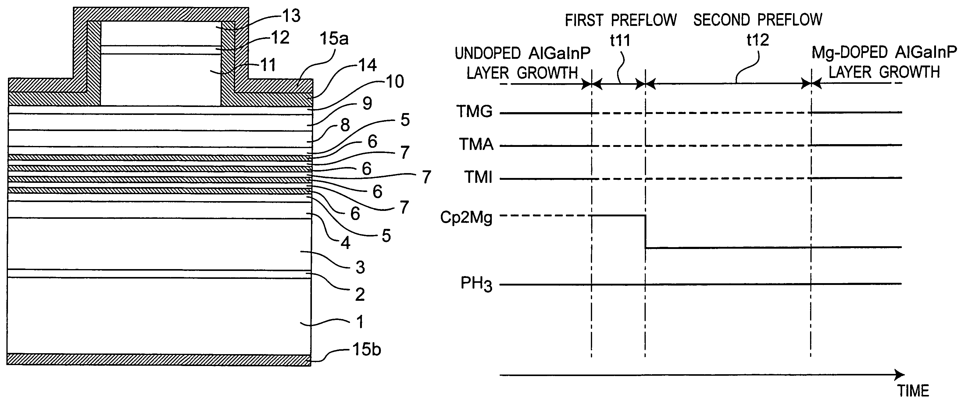
[0116]FIG. 1 shows the cross-sectional structure of a red light emitting AlGaInP based semiconductor laser device manufactured by the semiconductor laser device manufacturing method of one embodiment.

[0117]The semiconductor laser device includes an n-Ga0.508In0.492P interlayer (thickness: 0.25 μm) 2, an n-(Al0.684Ga0.316)0.511In0.489P first n-cladding layer (thickness: 2.6 μm) 3, an n-(Al0.7Ga0.3)0.511In0.489P second n-cladding layer (thickness: 0.2 μm) 4, an (Al0.545Ga0.455)0.511In0.489P guide layer (thickness: 35 nm) 5, a multiple quantum well layer active layer in which a Ga0.445In0.555P well layer (thickness: 5 nm) 6 and an (Al0.545Ga0.455)0.511In0.489P barrier layer (thickness: 6.3 nm) 7 are layered alternately in multiplicity, an undoped (Al0.7Ga0.3)0.511In0.489P cladding layer (thickness: 35 nm) 8, a p-(Al0.7Ga0.3)0.511In0.489P first p-cladding layer (thickness: 0.237 μm) 9, a p-Ga0.623In0.377P etching stop layer (thickness: 13 nm) 10, a p-(Al0.7Ga0.3)0.5...


PUM

PropertyMeasurementUnit
pressureaaaaaaaaaa
temperatureaaaaaaaaaa
thicknessaaaaaaaaaa

Abstract

There are provided preflow periods t11, t12 in which group III element materials TMG, TMA and TMI are not supplied from a group III element material container to a reaction region (reactor), while a group V element material PH3 and an Mg dopant material are supplied from a group V element material container and a dopant material container to the reaction region (reactor) after an Mg-undoped group III-V compound semiconductor layer is crystallinically grown and before an Mg-doped group III-V compound semiconductor layer is crystallinically grown. According to the semiconductor manufacturing method, an Mg doping profile can be accurately controlled.

Description

CROSS-REFERENCE TO RELATED APPLICATIONS[0001]This nonprovisional application claims priority under 35 U.S.C. §119(a) on Patent Application No(s). 2006-190274 filed in Japan on Jul. 11, 2006, the entire contents of which are hereby incorporated by reference.BACKGROUND OF THE INVENTION[0002]The present invention relates to a semiconductor manufacturing method and more particularly to a semiconductor manufacturing method for crystallinically growing a group III-V compound semiconductor using Mg as a dopant.[0003]The present invention also relates to a semiconductor laser device manufacturing method for manufacturing an AlGaInP based semiconductor laser device by using the semiconductor manufacturing method.[0004]In recent years, semiconductor laser devices of a group III-V compound semiconductor (e.g., AlGaInP) system as those used for DVD (Digital Versatile Disc) drives are required to have severe specifications of the capabilities of high efficiency, low operating voltage, good tempe...

Claims


Application Information

Patent Timeline
Patent Type & Authority Patents(United States)
IPC IPC(8): H01L21/00
CPCB82Y20/00H01S5/34326H01S5/22H01S2304/04H01S5/3063Y10S438/931
Inventor YAMAMOTO, KEINAKAMURA, JUNICHI
Owner SHARP KK
Why Eureka
Try Eureka