Power amplification device

a power amplifier and amplifier technology, applied in the direction of amplifiers with semiconductor devices only, amplifiers with semiconductor devices, amplifiers, etc., can solve the problem of limiting the magnitude of the drivable load, the precision of the sensitivity setting of the protection circuit cannot be sufficiently enhanced by conventional devices, and the output transistor cannot be destroyed. ambiguous determination, the effect of maximizing the detection sensitivity and load driving performance at the time of erroneous connection

Inactive Publication Date: 2009-07-07
KK TOSHIBA
View PDF8 Cites 8 Cited by
  • Summary
  • Abstract
  • Description
  • Claims
  • Application Information

AI Technical Summary

Benefits of technology

[0082]Even in the state (short-to-supply state) in which the output terminal 12-1 or output terminal 12-2 is short-circuited to the internal power supply Vcc, if the comparators C1 and C2 are configured as comparators for short-to-supply, the same advantageous effects can be obtained. Specifically, in the case of the comparators for short-to-supply, it should suffice if the determination by the comparator C1 and comparator C2 is altered to Pin(COMP)=Pm4−Pm1, if a description is given by using the formula (2). Thus, a detailed description of the short-to-supply state is omitted here.
[0083]According to the power amplification device of this embodiment, at least the following advantageous effects (1) to (3) can be obtained.
[0084](1) The detection sensitivity and load driving performance at the time of erroneous connection can be maximized.
[0086]As has been described above, the power amplification device 10 includes the power detection circuits D1 to D4 which detect the powers of the output transistors M1 to M4.
[0087]Whether the output transistor, M1 to M4, is destroyed or not is determined by whether a heat amount [heat W=power P=current I×voltage V], which is produced in the output transistor, M1 to M4, exceeds a predetermined tolerance value or not. In the conventional protection means, however, a current flowing in the output transistor is let to flow through a current-mirrored detection transistor, and the current is directly monitored, detected and compared. Thus, the conventional protection means is configured to detect only the current I among the factors that determine the heat amount. This being the case, only ambiguous determination can be made as to whether the output transistor is destroyed or not.
[0088]On the other hand, in the power amplification device 10 according to the present embodiment, the powers of the output transistors M1 to M4 can be detected by the power detection circuits D1 to D4. Thus, both factors, current I and voltage V, which determine the heat amount, can be detected, and the heat amount can be detected on the basis of the essential factors of the same order. Therefore, the detection sensitivity and load driving performance at the time of erroneous connection can be maximized.

Problems solved by technology

This being the case, there is a tendency that only ambiguous determination can be made as to whether the output transistor is destroyed or not.
As a result, the conventional device cannot sufficiently enhance the precision of sensitivity setting of the protection circuit, and is disadvantageous in improving the detection / protection sensitivity of short-to-ground or short-to-supply, thereby to prevent destruction of the amplifier circuit.
In short, the magnitude of the drivable load is restricted, and this is disadvantageous in maximizing the performance for driving the BLT load.

Method used


Image

  • Power amplification device
  • Power amplification device
  • Power amplification device

Examples


first embodiment

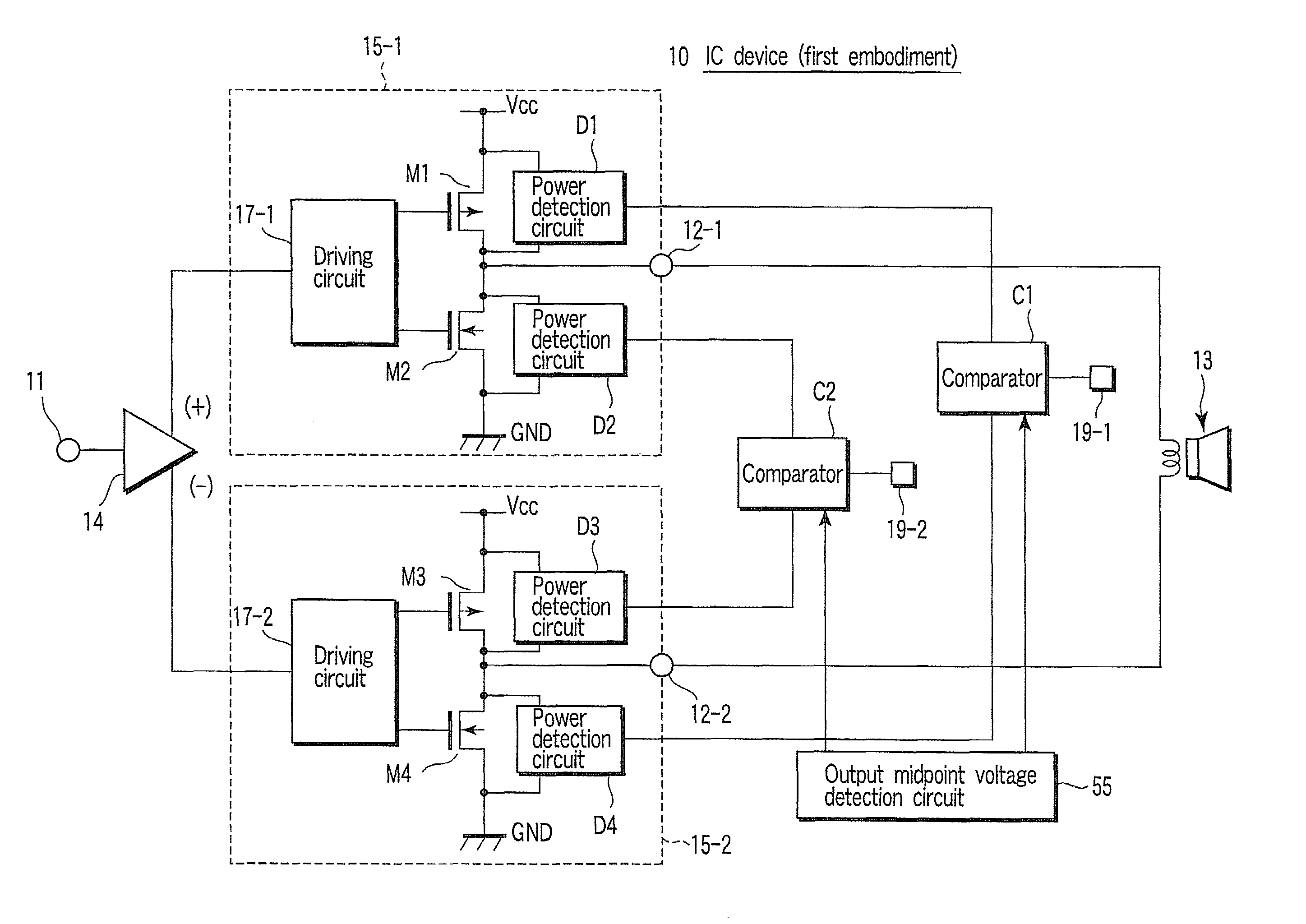
[0027]To begin with, referring to FIG. 1, a power amplification device according to a first embodiment of the present invention is described. FIG. 1 is a block diagram showing the power amplification device according to the first embodiment. In this embodiment, an amplification circuit device using a BTL (Bridge Tied Load) system is described by way of example.

[0028]As shown in FIG. 1, the power amplification device 10 includes a speaker 13, an amplifier 14, amplification circuits 15-1 and 15-2, comparators C1 and C2, and an output midpoint voltage detection circuit 55. The power amplification device 10 is configured to detect an overload state occurring at a time of short-to-ground or short-to-supply due to erroneous connection of an output terminal 12-1 or 12-2, while driving the speaker 13 by means of the BTL-system amplification circuits 15-1 and 15-2.

[0029]The amplifier 14 is configured to amplify an input signal from an input terminal 11, and to output the amplified signal to ...

example 1

An Example of the Power Detection Circuit

[0106]Next, a power amplification device according to Example 1 is described with reference to FIG. 8. Example 1 relates to an example of the power detection circuit D1. A detailed description of the parts common to those in the first embodiment is omitted here.

[0107]As shown in FIG. 8, the power detection circuit D1 includes a current-mirror transistor M11, resistors R11 and R12, and bipolar transistors Q11 and Q12 that constitute a current-mirror circuit.

[0108]The current-mirror transistor M11 is configured to detect a current of the output transistor M1. The current-mirror transistor M11 is a PMOS transistor having a source connected to the internal power supply Vcc, a drain connected to an emitter of the bipolar transistor Q1, and a gate connected to the gate of the output transistor M1.

[0109]One end of the resistor R11 is connected to the emitter of the bipolar transistor Q11, and the other end thereof is connected to an emitter of the b...

example 2

An Example of the Power Detection Circuit

[0115]Next, a power amplification device according to Example 2 is described with reference to FIG. 9. Example 2 relates to an example of the power detection circuit D2. A detailed description of the parts common to those in the first embodiment is omitted here.

[0116]As shown in FIG. 9, the power detection circuit D2 includes a current-mirror transistor M22, resistors R21 and R22, and bipolar transistors Q21 and Q22 that constitute a current-mirror circuit.

[0117]The current-mirror transistor M22 is configured to detect a current of the output transistor M2. The current-mirror transistor M22 has a source connected to the ground power supply GND, a drain connected to an emitter of the bipolar transistor Q21, and a gate connected to the gate of the output transistor M2.

[0118]One end of the resistor R21 is connected to the emitter of the bipolar transistor Q21, and the other end thereof is connected to an emitter of the bipolar transistor Q22. On...


PUM


Abstract

A power amplification device includes a BTL amplification circuit including a first amplification circuit and a second amplification circuit, the first amplification circuit including a first output transistor, a first power detection circuit, a second output transistor, and a second power detection circuit, the second amplification circuit including a third output transistor, a third power detection circuit, a fourth output transistor, and a fourth power detection circuit, a first comparator which compares output values of the first and fourth power detection circuits, and a second comparator which compares output values of the second and third power detection circuits.

Description

CROSS-REFERENCE TO RELATED APPLICATIONS[0001]This application is based upon and claims the benefit of priority from prior Japanese Patent Application No. 2006-271073, filed Oct. 2, 2006, the entire contents of which are incorporated herein by reference.BACKGROUND OF THE INVENTION[0002]1. Field of the Invention[0003]The present invention relates to a power amplification device, and is applied, for example, to a power amplification device using a BTL (Bridge Tied Load) system.[0004]2. Description of the Related Art[0005]Conventionally, there is known a BTL-system amplification device as a power amplification device that is used as an amplifier for a speaker of vehicle-mounted stereo equipment or other audio equipment (e.g. Jpn. Pat. Appln. KOKAI Publication No. 5-235652). As disclosed in KOKAI Publication No. 5-235652, a BTL-system amplifier circuit device includes a pair of amplification circuits (2) and (3), and thus both the voltage and current, which can be output to a speaker (4)...

Claims


Application Information

Patent Timeline
Patent Type & Authority Patents(United States)
IPC IPC(8): H02H7/20
CPCH03F1/523H03F3/2171H03F3/2173H03F2200/78H03F2200/465H03F2200/471H03F2200/03
Inventor TSURUMI, HIROYUKI
Owner KK TOSHIBA
Why Eureka
Try Eureka