Driving circuit for electro-optical device, method of driving electro-optical device, electro-optical device, and electronic apparatus

a technology of driving circuit and electrooptical device, applied in the direction of static indicating device, cathode-ray tube indicator, instruments, etc., can solve problems such as inability to perceiv

Inactive Publication Date: 2009-07-07
138 EAST LCD ADVANCEMENTS LTD
View PDF16 Cites 13 Cited by
  • Summary
  • Abstract
  • Description
  • Claims
  • Application Information

AI Technical Summary

Benefits of technology

[0008]An advantage of the invention is that it provides a driving circuit for an electro-optical device capable of performing uniform display, a method of driving an electro-optical device, an electro-optical device, and an electronic apparatus having an electro-optical device.
[0009]According to a first aspect of the invention, there is provided a driving circuit for an electro-optical device which drives an electro-optical device having a plurality of data lines and a plurality of scanning lines extending so as to cross each other and a plurality of pixel units connected to the scanning lines and the data lines to form a display surface. The driving circuit for an electro-optical device includes a memory into / from which image signals are written / read, the image signals being for performing gray scale display in the plurality of pixel units, a scanning line driving unit that selects the scanning lines and supplies scanning signals to the selected scanning lines, a data line driving unit that selects the data lines and supplies the image signals read out from the memory to the selected data lines, and a control unit that controls an operation of at least one of the scanning line driving unit and the data line driving unit, such that at least one of a selection sequence of the plurality of scanning lines and a selection sequence of the plurality of data lines is inverted at a predetermined inversion cycle, and that controls writing and reading of the image signals in the memory, such that the image signals written into the memory are read out in a state in which an arrangement sequence of the image signals is inverted at the inversion cycle.
[0010]In accordance with the first aspect of the invention, when driving, one or both of the selection sequence of the scanning lines and the selection sequence of the data lines are inverted at the predetermined cycle. The ‘selection’ described herein means that one pixel unit is selected to be supplied with the image signal in a so-called matrix driving method. A voltage is applied to the selected scanning line and a row of pixels is selected. In addition, the image signal is supplied to the selected data line, such that a writing operation is performed with respect to one pixel unit among the row of pixels.
[0011]Specifically, one or both of a direction in which the scanning signals are supplied to the scanning lines, that is, a vertical scanning direction (hereinafter, referred to as ‘a vertical scanning direction’) and a direction in which the image signals are supplied to the data lines, that is, a horizontal scanning direction (hereinafter, referred to as ‘a horizontal scanning direction’) are inverted at the predetermined cycle. For example, the data line driving unit supplies the image signals in a sequence from the left side of the screen to the right side thereof in an odd-numbered screen and supplies the image signals in a sequence from the right side of the screen to the left side thereof in an even-numbered screen. In addition, the scanning line driving unit sequentially supplies the scanning signals in a sequence from the upper side of the screen to the lower side thereof in the odd-numbered screen and sequentially supplies the scanning signals in a sequence from the lower side of the screen to the upper side thereof in the even-numbered screen. That is, the horizontal scanning direction or the vertical scanning direction is inverted for each screen.
[0012]The directions in which the signals are supplied from one or both of the scanning line driving unit and the data line driving unit are controlled by the control unit to be inverted. At this time, the control unit inverts the signal supply direction at the predetermined inversion cycle, for example, for each screen. For this reason, the difference in ghost in a horizontal direction of the screen or dark spots in a vertical direction thereof are averaged on the time axis, thereby performing a uniform display.
[0013]Here, the control unit may be constructed as a controller that controls the operation of the entire driving circuit or may be additionally provided in the driving unit as an inversion operation control unit. In addition, a portion that controls the inversion operation of the signal supply direction and a portion that controls the inversion operation in the memory may be separately provided. In addition, ‘the inversion cycle’ may be suitably set within a range in which the inversion of the signal supply direction may be actually performed, for example, in terms of frames, fields, or lines.

Problems solved by technology

Similarly, even though display irregularities occur due to ‘supply direction inversion driving’, it cannot be perceived.

Method used


Image

  • Driving circuit for electro-optical device, method of driving electro-optical device, electro-optical device, and electronic apparatus
  • Driving circuit for electro-optical device, method of driving electro-optical device, electro-optical device, and electronic apparatus
  • Driving circuit for electro-optical device, method of driving electro-optical device, electro-optical device, and electronic apparatus

Examples


first embodiment

1: First Embodiment

[0060]An electro-optical device according to a first embodiment of the invention will be described with reference to FIGS. 1 to 8B.

1-1: Configuration of Liquid Crystal Device

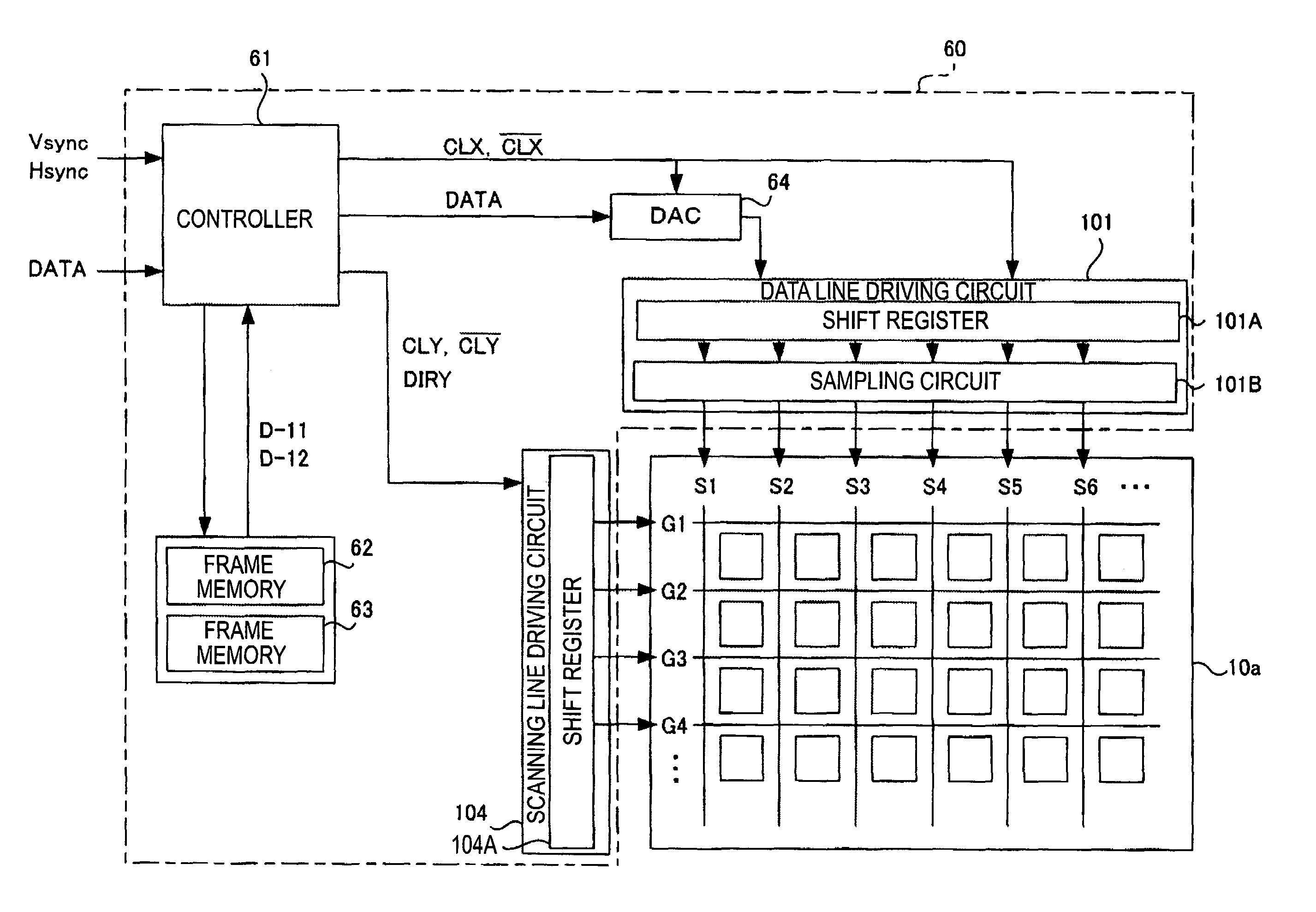
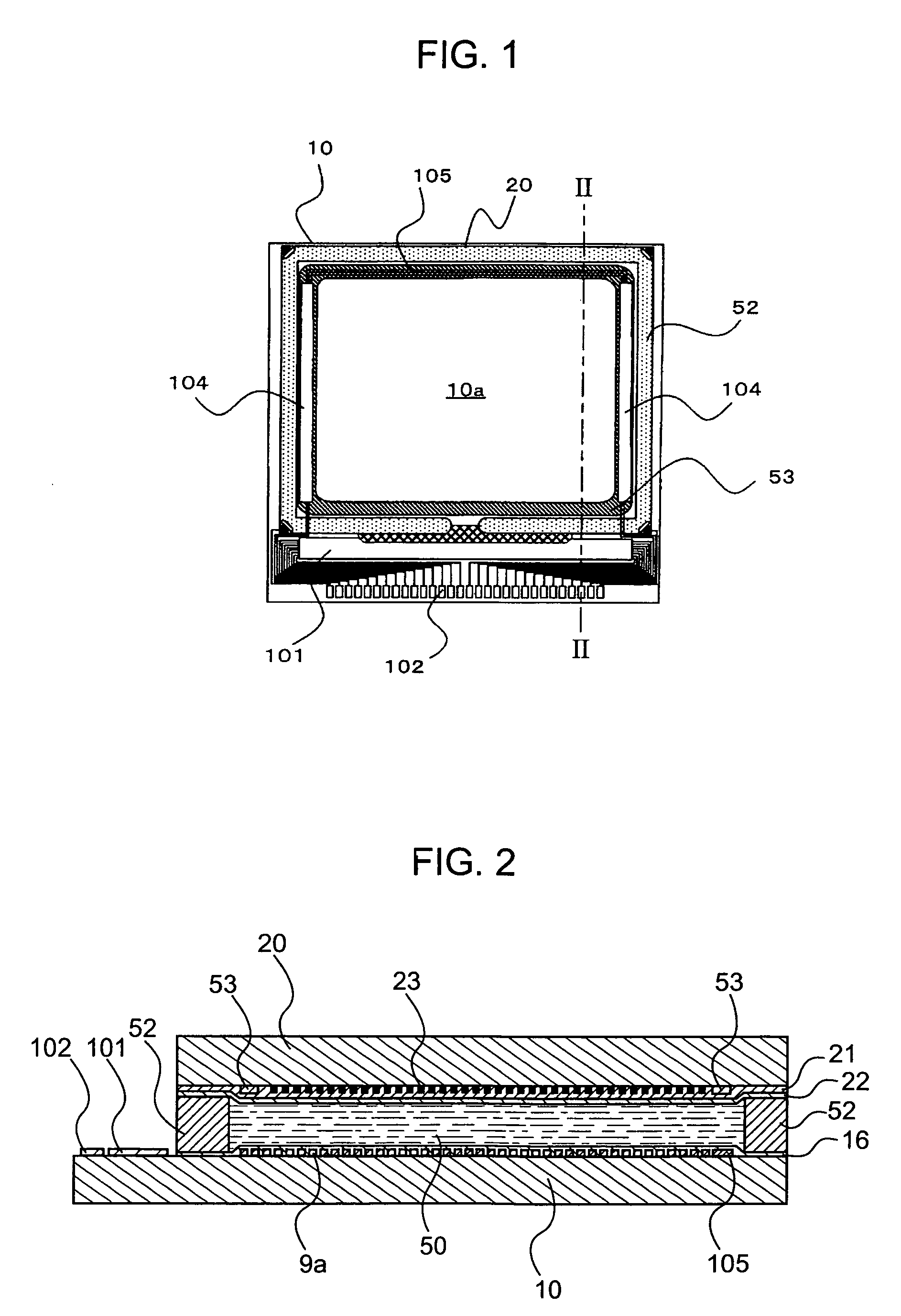
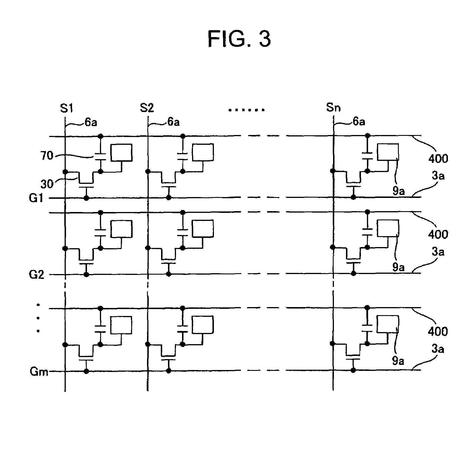
[0061]First, the configuration of a liquid crystal device, which is an electro-optical device according to the present embodiment, will be described with reference to FIGS. 1 to 4. FIG. 1 is a plan view showing an external configuration of the liquid crystal device. FIG. 2 is a cross-sectional view taken along the line II-II of FIG. 1. FIG. 3 is an equivalent circuit diagram of pixel units in the liquid crystal device, and FIG. 4 is a block diagram of a driving system including a driving circuit unit.

[0062]In FIG. 1, the liquid crystal device has a configuration in which a liquid crystal layer 50 is interposed between a TFT array substrate 10 and a counter substrate 20 arranged to face each other. That is, as one specific example of the invention, in the liquid crystal device, a TFT active-mat...

second embodiment

2: Second Embodiment

[0088]An electro-optical device according to a second embodiment of the invention will be described with reference to FIGS. 9 to 12B. FIG. 9 is a block diagram showing the configuration of a driving system including driving circuit units in the electro-optical device according to the second embodiment. FIG. 10 is a diagram conceptually showing a driving method according to the present embodiment. FIG. 11 is a timing chart according to the driving method of the present embodiment. FIGS. 12A and 12B are diagrams showing a sequence of a signal inversion process by frame memories 62 and 63. Moreover, the configuration and the driving method of the liquid crystal device according to the second embodiment are the same as those in the first embodiment. Thus, the same constituents as those in the first embodiment will be represented by the same reference numerals and the descriptions thereof will be omitted.

[0089]In the first embodiment, the driving method is described i...

third embodiment

3: Third Embodiment

[0099]An electro-optical device according to a third embodiment of the invention will be described with reference to FIGS. 13 and 14B. FIG. 13 is a diagram conceptually showing a driving method according to the present embodiment. FIGS. 14A and 14B are diagrams illustrating a sequence of a signal inversion process by frame memories 62 and 63.

[0100]In FIG. 13, in a liquid crystal device according to the present embodiment, both a horizontal scanning direction and a vertical scanning direction are inverted for each screen when driving. This driving method can be achieved through the following process. The controller 61 outputs to the scanning line driving circuit 104 and the data line driving circuit 101 the direction signals DIRX and DIRY, the values of which are inverted at a unit period cycle. At this time, an output sequence of the shift register 104A (that is, the output sequence of the scanning signals G1, G2, . . . , and Gm with respect to the scanning lines ...


PUM


Abstract

A driving circuit for an electro-optical device, that drives an electro-optical device having a plurality of data lines and a plurality of scanning lines extending so as to cross each other and a plurality of pixel units connected to the scanning lines and the data lines to form a display surface, includes a memory into / from which image signals are written / read, such that the plurality of pixel units perform grayscale display, a scanning line driving unit that selects the scanning lines and supplies scanning signals to the selected scanning lines, a data line driving unit that selects the data lines and supplies the image signals read out from the memory to the selected data lines, and a control unit that controls an operation of at least one of the scanning line driving unit and the data line driving unit, such that at least one of a selection sequence of the plurality of scanning lines and a selection sequence of the plurality of data lines is inverted at a predetermined inversion cycle, and that controls writing and reading of the image signals in the memory, such that the image signals written into the memory are read out in a state in which an arrangement sequence of the image signals is inverted at the inversion cycle.

Description

BACKGROUND OF THE INVENTION[0001]1. Technical Field[0002]The present invention relates to a driving circuit for an electro-optical device mounted on an electro-optical device, such as a liquid crystal device, to a method of driving an electro-optical device, to an electro-optical device, and to an electronic apparatus having an electro-optical device.[0003]2. Related Art[0004]Generally, a driving circuit is incorporated into a substrate of an electro-optical device, such as a liquid crystal device, so as to function as a data line driving circuit for driving data lines or a scanning line driving circuit for driving scanning lines. During operation, image signals are supplied to a row of pixel units, which is selected through vertical scanning by a scanning line driving unit, via the data lines from a-data line driving unit, such that data is written into the pixel units.[0005]In a driving method, various methods for reducing display defects which occur during driving have been conce...

Claims


Application Information

Patent Timeline
Patent Type & Authority Patents(United States)
IPC IPC(8): G09G3/36
CPCG09G3/3648G09G5/399G09G2340/0435G09G2310/0283G09G2320/0247G09G2310/02
Inventor TOKUMURA, TOSHIAKI
Owner 138 EAST LCD ADVANCEMENTS LTD
Why Eureka
Try Eureka