Magnetic field sensor provided with an upper shield layer having portions with different magnetostriction
a magnetic field sensor and shield layer technology, applied in the field of magnetic field sensors, can solve the problems of unstable magnetization of the upper shield layer caused by these effects, difficulty in applying the desired bias magnetic field, and affecting the free layer, etc., to achieve stable magnetization of the upper shield layer, stable output characteristics, and simple structure
- Summary
- Abstract
- Description
- Claims
- Application Information
AI Technical Summary
Benefits of technology
Problems solved by technology
Method used
Image
Examples
first embodiment
The First Embodiment
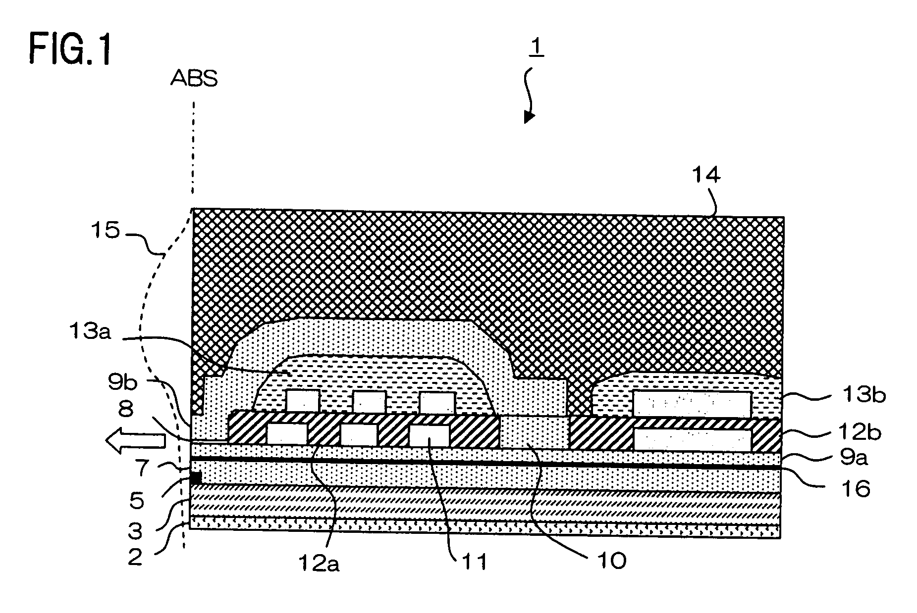
[0049]The first embodiment of a magnetic field sensor of the present invention will be described in detail with reference to the drawings. FIG. 1 is a partial sectional view of a thin-film magnetic head having a magnetic field sensor of the present invention. Thin-film magnetic head 1 has a substrate, not shown, that is made of ceramic, such as AlTiC (Al2O3.TiC), and layers beginning from seed layer 2 to protective layer 14 which are stacked in this order, as will be described later.
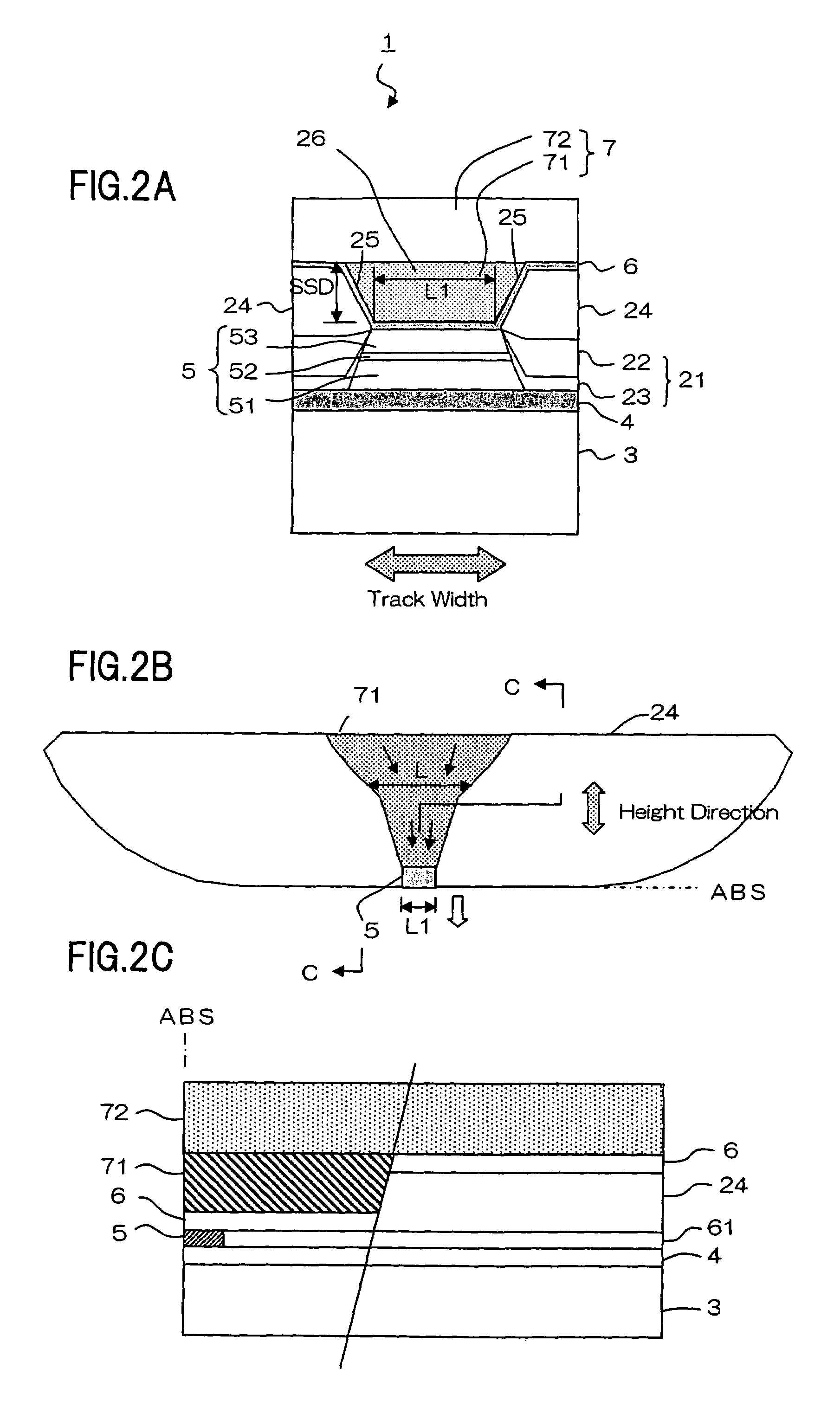
[0050]Specifically, lower shield layer 3 made of perm-alloy (NiFe) is formed on the substrate, with seed layer 2 made of alumina (Al2O3) interposed therebetween. Lower shield layer 3 functions as a lower magnetic shield layer for the reproducing head, or MR element 5 which functions as a magnetic field detecting element. MR element 5 is formed on lower shield layer 3 on the side of the air bearing surface (ABS), which is the surface of thin-film magnetic head 1 that faces a recording ...
second embodiment
The Second Embodiment
[0072]Next, the second embodiment of a thin-film magnetic head of the present invention will be described. Since this embodiment is the same as the first embodiment except for the configurations of the first portion and the lead electrodes, the description will focus on the configurations of the first portion and the lead electrodes.
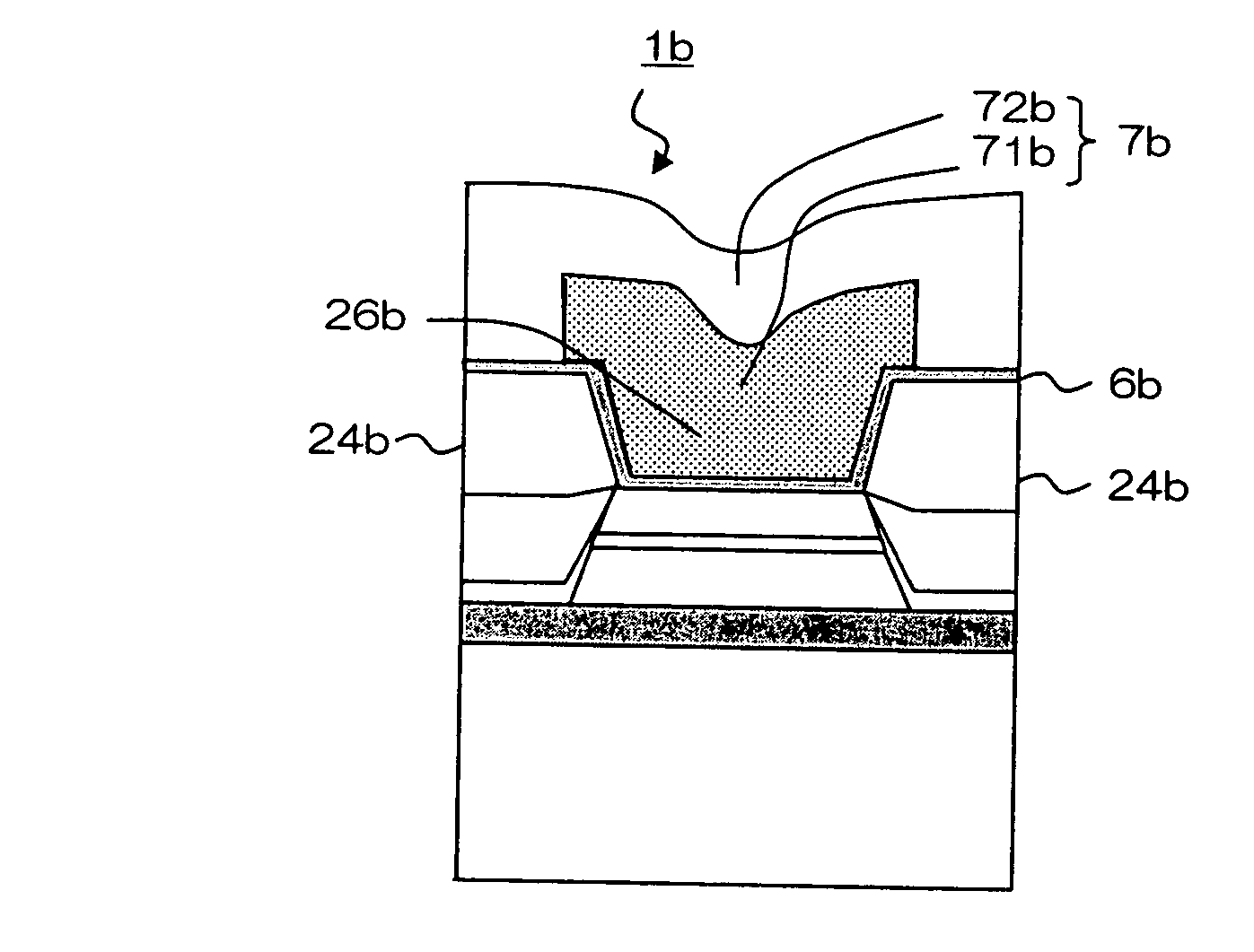
[0073]FIG. 5A is a side view of a thin-film magnetic head, viewed from ABS. FIG. 5B is a partial plan view showing the location near the MR element and the lead electrodes. Upper shield layer 7d includes first portion 71d and second portion 72d. First portion 71d is formed such that it fills only recess 26d and extends in approximately the same cross section along the height direction. This configuration corresponds to the configuration of lead electrodes 24d in which the electrodes extend along the height direction with approximately the same spacing therebetween. Such a configuration in which the first portion 71d is elongate in th...
third embodiment
The Third Embodiment
[0074]Next, the third embodiment of a thin-film magnetic head of the present invention will be described. Since this embodiment is the same as the first embodiment except for the configurations of the first portion and the lead electrodes, the description will focus on the configurations of the first portion and the lead electrodes.
[0075]FIG. 6A is a side view of a thin-film magnetic head, viewed from ABS. FIG. 6B is a partial plan view showing the location near an MR element and lead electrodes. FIG. 6C is a sectional view taken along line C-C in FIG. 6B. A pair of lead electrodes 24e are provided on both sides of MR element 5 with respect to the track width direction. Upper gap layer 6e extends to cover the opposing surfaces of the pair of lead electrodes 24e, as well as MR element 5. As a result, recess 26e is formed between the opposing surfaces of upper gap layer 6e. Upper shield layer 7e has first portion 71e and second portion 72e. First portion 71e, diffe...
PUM
| Property | Measurement | Unit |
|---|---|---|
| thickness | aaaaa | aaaaa |
| depth | aaaaa | aaaaa |
| depth | aaaaa | aaaaa |
Abstract
Description
Claims
Application Information


