
Film taking-off method

a film and film technology, applied in the field of film production, can solve the problems of complex and expensive reclaiming operation proposed by u.s. patent no. 6,596,610, and may manifest particle contamination problems, and achieve the effects of simple and fast reclaiming operation, low cost, and good crystalline quality

Active Publication Date: 2009-08-11
SOITEC SA
View PDF26 Cites 4 Cited by
  • Summary
  • Abstract
  • Description
  • Claims
  • Application Information

AI Technical Summary

Benefits of technology

[0015]The invention now provides a method to remove and transfer a film from a wafer in such a way that the film is of good crystalline quality and has regular borders, with minimal contamination. It also enables reclaiming of the wafer that has provided the film, so that it can again provide additional films with minimum risk of contamination.
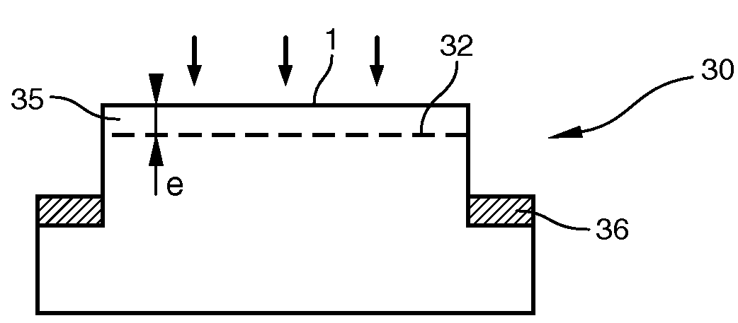
[0016]According to one embodiment, the invention relates to a method of producing a film for electronic, optic or optronic applications from a wafer, by forming a step of defined height around the periphery of the wafer, with the step having a mean thickness that is less than that of the wafer; and selectively implanting atomic species through a face of the wafer but not through the step to form an implanted zone at a defined implant depth with the film being defined between the face of the wafer and the implanted zone. The implantation of atomic species into the step can be prevented by forming a protective layer at least over the step or by masking the step.

Problems solved by technology

This particle contamination problem may also be manifested during the “reclaiming” treatments needed to reform a clean film, which can subsequently be transferred.
However, the reclaiming operation proposed by U.S. Pat. No. 6,596,610 remains complex and expensive as it requires a selective treatment of the ring, and this treatment must also be repeated at each taking-off.

Method used


Image

  • Film taking-off method
  • Film taking-off method
  • Film taking-off method

Examples


example 1

Formation of the Protective Layer 36

[0088]LPCVD deposition of a thin SiO2 layer;

[0089]anisotropic etching, such as RIE etching, in order to remove the protective material present on the front face 1.

example 2

Formation of the Protective Layer 36

[0090]PECVD deposition of SiO2 or Si3N4, optionally preceded by a thin thermal oxidation; a thickness of Rp+5*ΔRp (see above) or greater may be chosen. Thus, by adjusting the thickness of the layer 36′ it is possible to minimize the amount of material to be deposited, and therefore the cost of the operation; and

[0091]CMP (Chemical-Mechanical Planarization) polishing on at least the front face 1 in order to remove the SiO2 or Si3N4 layer selectively over the subjacent material.

example 3

Formation of the Protective Layer 36

[0092]thermal oxidation of the wafer 30; and

[0093]CMP polishing on at least the front face 1 in order to remove the SiO2 and Si3N4 layer selectively over the subjacent material.


PUM


Abstract

The invention relates to a method of producing a film intended for applications in electronics, optics or optronics starting from an initial wafer, which includes a step of implanting atomic species through one of the faces of the wafer. This method includes forming a step of defined height around the periphery of the wafer, with the step having a mean thickness that is less than that of the wafer; and selectively implanting atomic species through a face of the wafer but not through the step to form an implanted zone at a defined implant depth with the film being defined between the face of the wafer and the implanted zone. The implantation of atomic species into the step can be prevented by forming a protective layer at least over the step or by masking the step. The invention also relates to a wafer obtainable by the method.

Description

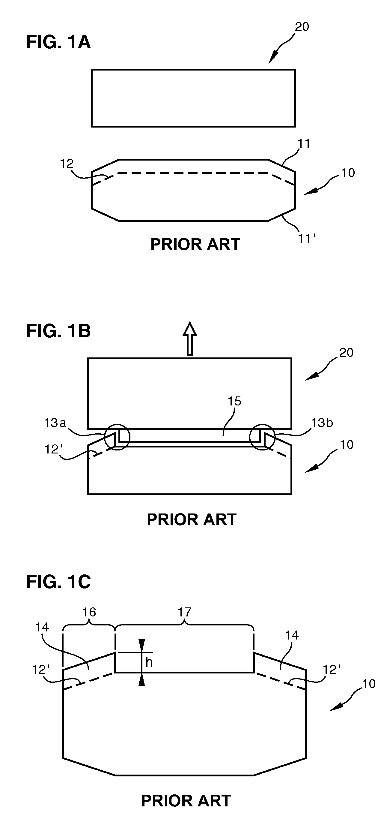
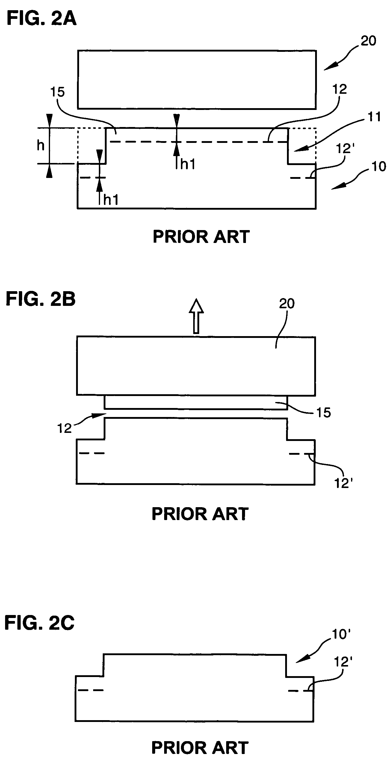
BACKGROUND OF THE INVENTION[0001]The present invention relates to the production of a film, starting from an initial wafer, including a step of implanting atomic species through one of its faces in order to form therein a buried implanted zone at a defined depth, with the film to be produced then being bounded by the implanted face of the wafer and by this implanted zone.[0002]This technique is especially employed for lifting off the film, by carrying out, after the implantation, the following steps (illustrated by FIGS. 1A and 1B):[0003]the wafer 10 is bonded on its implanted face to a receiving substrate 20; and[0004]energy (typically thermal and / or mechanical energy) is supplied so as to detach the film 15 from the implanted zone 12 (this process is known in the art by the term SMART-CUT®).[0005]The film 15 is then taken off the wafer 10, to be transferred onto the receiving substrate 20 (see FIG. 1B).[0006]Referring to FIGS. 1A and 1B, the faces of the wafer 10 are usually chamf...

Claims


Application Information

Patent Timeline
Patent Type & Authority Patents(United States)
IPC IPC(8): H01L21/30
CPCH01L21/76254
Inventor AULNETTE, CECILECAYREFOURCQ, IANMAZURE, CARLOS
Owner SOITEC SA
Learn More