

Apparatus and methods for adjusting an edge ring potential substrate processing
- Summary
- Abstract
- Description
- Claims
- Application Information
AI Technical Summary
Benefits of technology
Problems solved by technology
Method used
Image

Examples
Embodiment Construction
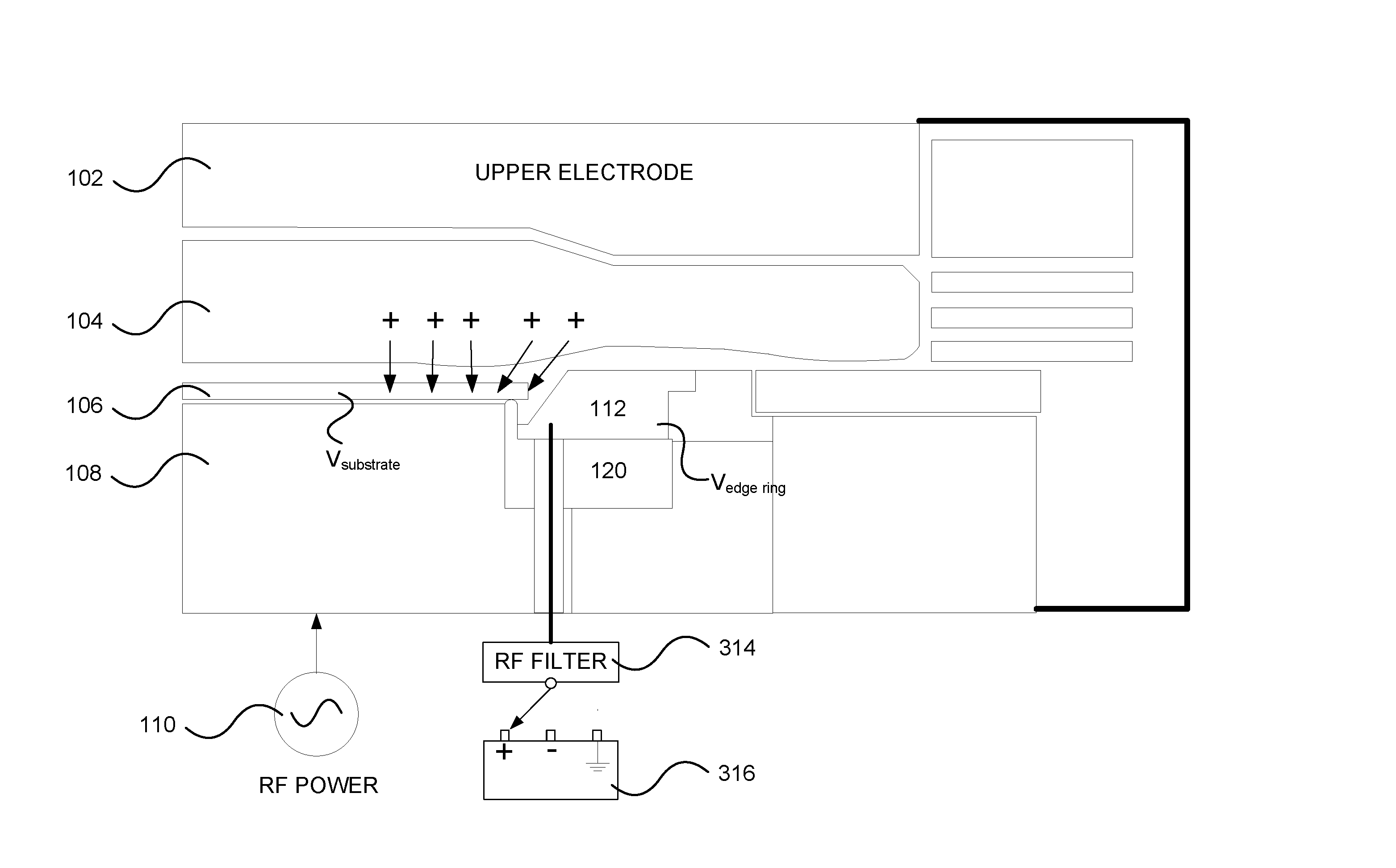
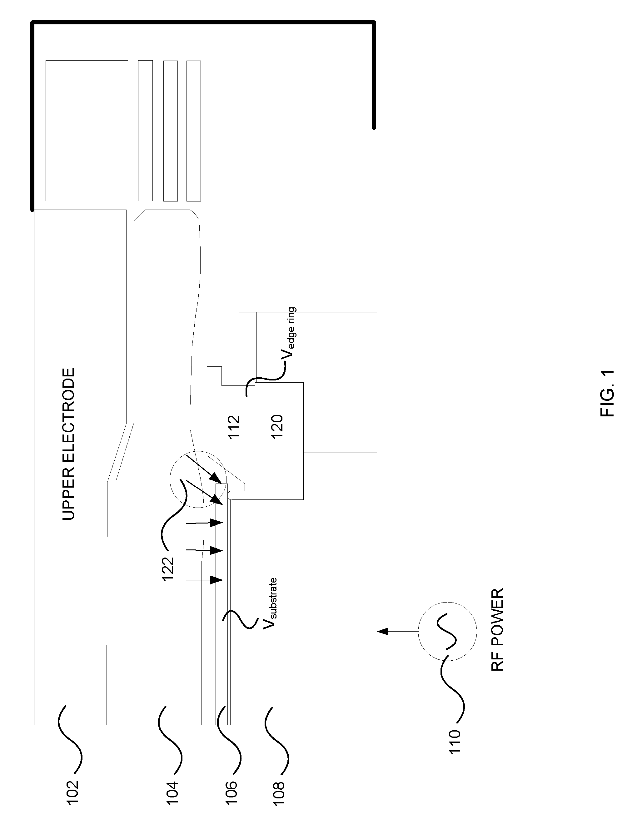
[0019]The present invention will now be described in detail with reference to a few preferred embodiments thereof as illustrated in the accompanying drawings. In the following description, numerous specific details are set forth in order to provide a thorough understanding of the present invention. It will be apparent, however, to one skilled in the art, that the present invention may be practiced without some or all of these specific details. In other instances, well known process steps and / or structures have not been described in detail in order to not unnecessarily obscure the present invention.
[0020]While not wishing to be bound by theory, the inventor believes that the ion angular distribution may be controlled by altering the DC potential between the substrate and the edge ring, thus optimizing the equipotential lines of the plasma sheath for a given plasma process. In an advantageous manner, changes may be made to the electric field around the substrate edge by changing an RF...
PUM
| Property | Measurement | Unit |
|---|---|---|
| Frequency | aaaaa | aaaaa |
| Frequency | aaaaa | aaaaa |
| Frequency | aaaaa | aaaaa |
Abstract
Description
Claims
Application Information