Fin structure and method of manufacturing fin transistor adopting the fin structure

a technology of fin transistor and fin structure, which is applied in the direction of basic electric elements, electrical apparatus, and semiconductor devices, can solve the problems of cost and manufacturing structure of fin transistor, and achieve the effect of high reliability and low cos

Active Publication Date: 2009-08-18
SAMSUNG ELECTRONICS CO LTD
View PDF7 Cites 128 Cited by
  • Summary
  • Abstract
  • Description
  • Claims
  • Application Information

AI Technical Summary

Benefits of technology

[0007]The present invention provides a method of uniformly forming an inexpensive, highly reliable fin structure and a method of manufacturing a fin transistor adopting the fin structure.

Problems solved by technology

In these conventional methods, with a narrow line width, uniformity of a fin structure is lowered, and it is costly to manufacture the fin structure.

Method used


Image

  • Fin structure and method of manufacturing fin transistor adopting the fin structure
  • Fin structure and method of manufacturing fin transistor adopting the fin structure
  • Fin structure and method of manufacturing fin transistor adopting the fin structure

Examples


Embodiment Construction

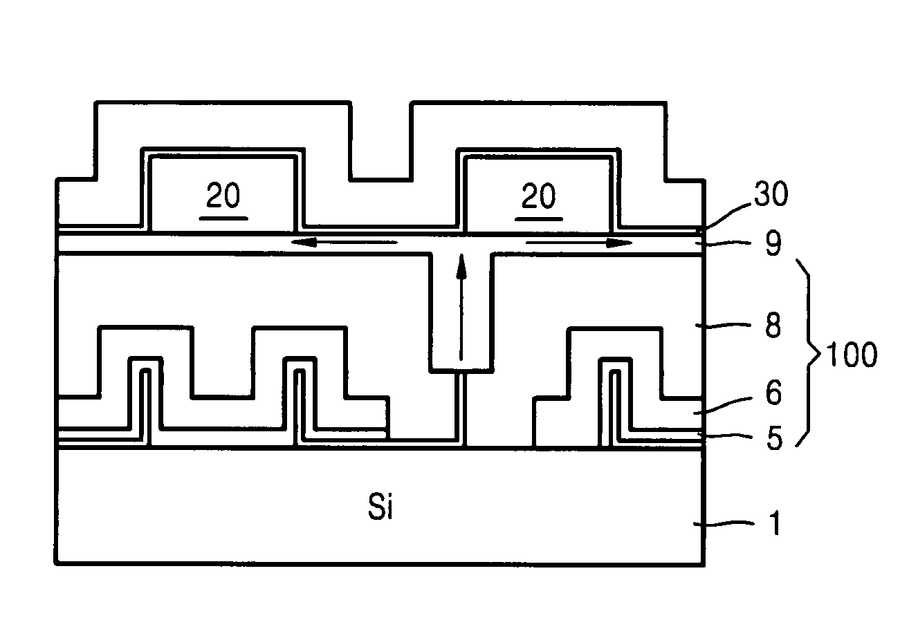
[0022]A method of manufacturing a fin structure according to the present invention will now be described with reference to the attached drawings. The method corresponds to a method of manufacturing a fin type active region of a fin transistor. Therefore, a method of manufacturing a fin transistor according to the present invention will be easily understood according to the method.

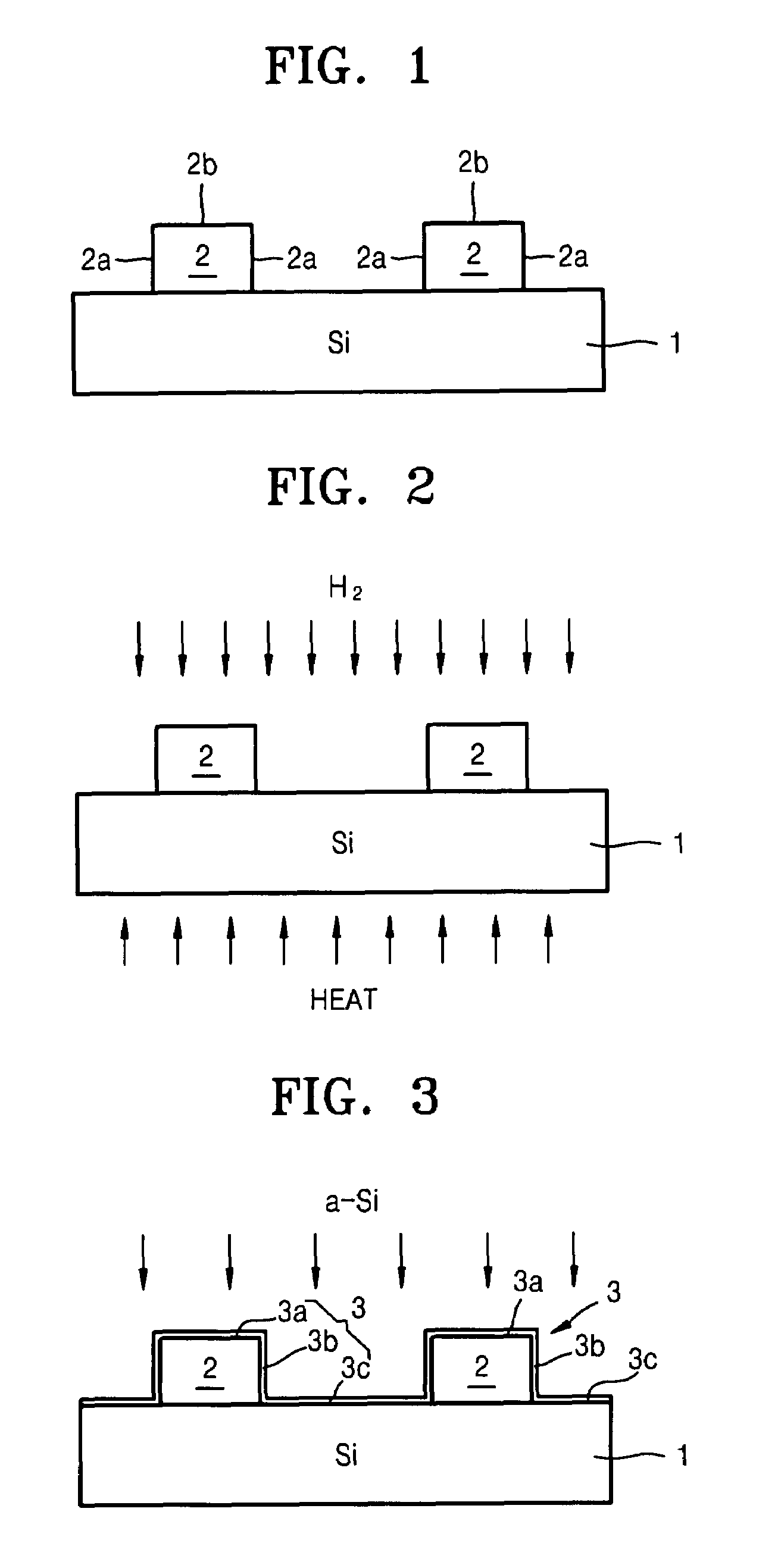
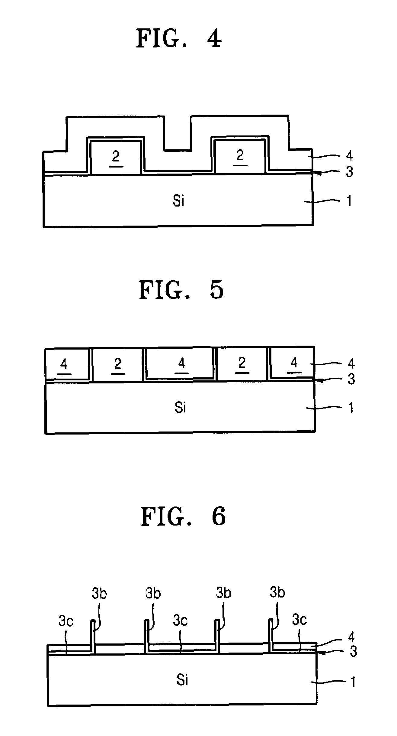
[0023]FIGS. 1 through 6 are cross-sectional views illustrating processes of manufacturing a fin structure according to an embodiment of the present invention. In embodiments of the present invention, silicon will be described as an application of a material of which a semiconductor layer is formed.

[0024]As shown in FIG. 1, a plurality of mesa structures 2 having predetermined lengths are formed on a silicon substrate 1. The mesa structures 2 have upper surfaces 2b and sides 2a formed besides the upper surfaces 2b. A distance between the mesa structures 2 must be appropriately adjusted according to a distanc...


PUM


Abstract

Provided are a fin structure and a method of manufacturing a fin transistor adopting the fin structure. A plurality of mesa structures including sidewalls are formed on the substrate. A semiconductor layer is formed on the mesa structures. A capping layer is formed on the semiconductor layer. Thus, the semiconductor layer is protected by the capping layer and includes a portion which is to be formed as a fin structure. A portion of an upper portion of the capping layer is removed by planarizing, and thus a portion of the semiconductor layer on upper surfaces of the mesa structures is removed. As a result, fin structures are formed on sides of the mesa structures to be isolated from one another. Therefore, a fin structure having a very narrow width can be formed, and a thickness and a location of the fin structure can be easily controlled.

Description

CROSS-REFERENCE TO RELATED PATENT APPLICATION[0001]This application claims the benefit of Korean Patent Application No. 10-2006-0076210, filed on Aug. 11, 2006, in the Korean Intellectual Property Office, the disclosure of which is incorporated herein in its entirety by reference.BACKGROUND OF THE INVENTION[0002]1. Field of the Invention[0003]The present invention relates to a method of manufacturing a fin structure, and more particularly, to a method of manufacturing a fin transistor used in a semiconductor memory device.[0004]2. Description of the Related Art[0005]Fin transistors are suitable for design rule of 100 nm or less. In particular, fin transistors have been researched as low-powered, high-efficient, and high-speed devices. Active regions having extremely line widths of 20 nm or less are required to obtain full depletions of the fin transistors. In order to obtain fin transistors satisfying this requirement, it is very important to manufacture fin structures that are acti...

Claims


Application Information

Patent Timeline
Patent Type & Authority Patents(United States)
IPC IPC(8): H01L21/00H01L21/84
CPCH01L27/105H01L27/1052H01L29/785H01L29/66795H10B99/00H01L21/18
Inventor CHO, HANS S.PARK, YOUNG-SOOXIANYU, WENXU
Owner SAMSUNG ELECTRONICS CO LTD
Why Eureka
Try Eureka